|
SEMI Book-to-Bill Historic Press Release Data �i�P�X�X�V�N�P���`�Q�O�O�S�N�P�P��) |
|||||||||||||||||||||||||||||||||||||||||||||||||||||||||||||||||||||||||||||||||||||||||||||||||||||||||||||||||||||||||||||||||||||||||||||||||||||||||||||||||||||||||
 |
|||||||||||||||||||||||||||||||||||||||||||||||||||||||||||||||||||||||||||||||||||||||||||||||||||||||||||||||||||||||||||||||||||||||||||||||||||||||||||||||||||||||||
���s�n�o |
|||||||||||||||||||||||||||||||||||||||||||||||||||||||||||||||||||||||||||||||||||||||||||||||||||||||||||||||||||||||||||||||||||||||||||||||||||||||||||||||||||||||||
|
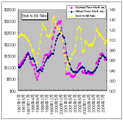
NORTH AMERICAN SEMICONDUCTOR EQUIPMENT INDUSTRY POSTS NOVEMBER 2004 BOOK-TO-BILL RATIO OF 1.00 |
|||||||||||||||||||||||||||||||||||||||||||||||||||||||||||||||||||||||||||||||||||||||||||||||||||||||||||||||||||||||||||||||||||||||||||||||||||||||||||||||||||||||||
| SAN JOSE, Calif., December 16, 2004 -- North American-based manufacturers
of semiconductor equipment posted $1.35 billion in orders in November 2004
(three-month average basis) and a book-to-bill ratio of 1.00 according
to the November 2004 Book-to-Bill Report published today by SEMI. A book-to-bill
of 1.00 means that $100 worth of orders were received for every $100 of
product billed for the month. The three-month average of worldwide bookings in November 2004 was $1.35 billion. The bookings figure is two percent below the revised October 2004 level of $1.37 billion and 46 percent above the $923 million in orders posted in November 2003. The three-month average of worldwide billings in November 2004 was $1.34 billion. The billings figure is six percent below the revised October 2004 level and 53 percent above the November 2003 billings level of $876 million. "Total orders for semiconductor equipment have declined about 16 percent from the peak observed in June of this year, though they remain well above levels reported one year ago," said Stanley T. Myers, president and CEO of SEMI. "The North American equipment Book-to-Bill ratio increased in November as billings declined at a steeper pace than bookings based on a three month average." The SEMI book-to-bill is a ratio of three-month moving averages of worldwide bookings and billings for North American-based semiconductor equipment manufacturers. Billings and bookings figures are in millions of U.S. dollars. |
|||||||||||||||||||||||||||||||||||||||||||||||||||||||||||||||||||||||||||||||||||||||||||||||||||||||||||||||||||||||||||||||||||||||||||||||||||||||||||||||||||||||||
|
|||||||||||||||||||||||||||||||||||||||||||||||||||||||||||||||||||||||||||||||||||||||||||||||||||||||||||||||||||||||||||||||||||||||||||||||||||||||||||||||||||||||||
| The data contained in this release was compiled by David Powell, Inc.,
an independent financial services firm, without audit, from data submitted
directly by the participants. SEMI and David Powell, Inc. assume no responsibility for the accuracy of the underlying data. The data are contained in a monthly Book-to-Bill Report published by SEMI. The report tracks billings and bookings worldwide of North American-headquartered manufacturers of equipment used to manufacture semiconductor devices, not billings and bookings of the chips themselves. SEMI is a global industry association serving companies that develop and provide manufacturing technology and materials to the global semiconductor, flat panel display, MEMS and related microelectronics industries. SEMI maintains offices in Austin, Beijing, Brussels, Hsinchu, Moscow, San Jose (Calif.), Seoul, Shanghai, Singapore, Tokyo and Washington, D.C. For more information, visit www.semi.org. ASSOCIATION CONTACTS: Dan Tracy/SEMI Tel: 1.408.943.7987 E-mail: dtracy@semi.org Jonathan Davis/SEMI Tel: 1.408.943.6937 E-mail: jdavis@semi.org |
|||||||||||||||||||||||||||||||||||||||||||||||||||||||||||||||||||||||||||||||||||||||||||||||||||||||||||||||||||||||||||||||||||||||||||||||||||||||||||||||||||||||||
���s�n�o |
|||||||||||||||||||||||||||||||||||||||||||||||||||||||||||||||||||||||||||||||||||||||||||||||||||||||||||||||||||||||||||||||||||||||||||||||||||||||||||||||||||||||||
|
FPD�֘A�Y�Ƃ̍��یo�c�҉�c �uGFPC�iGlobal FPD Partners Conference�j2005�v �Q�����\�����ݎ�t�J�n 2005�N2��27���i���j�`3��2���i���j�A���ꌧ����s�ɂĊJ�� |
|||||||||||||||||||||||||||||||||||||||||||||||||||||||||||||||||||||||||||||||||||||||||||||||||||||||||||||||||||||||||||||||||||||||||||||||||||||||||||||||||||||||||
| SEMI�iSemiconductor Equipment and Materials International�j�́A2005�N2��27���i���j-3��2���i���j��4���ԁA���ꌧ����s�̖����×��فi�������傤����j�ɂāAFPD�֘A�Y�Ƃ̍��یo�c�҉�c�uGFPC (Global FPD Partners Conference, �O���[�o��FPD�p�[�g�i�[�Y��c) 2005�v���J�Â��܂��B �uGFPC�v�́AFPD�p�l������ѐ������u�E�ޗ��ƊE�Ɗ֘A�ƊE�̌o�c�����w�ɂ��W�܂肢�������A�r�W�l�X�E�����E�Z�p�Ȃǂɂ����鋤�ʉۑ�𗦒��ɋc�_���AFPD�ƊE�̏����ɂނ����r�W�������l�����A�܂��A�C���t�H�[�}���ȕ��͋C�̒��ŁA���ꂼ��̃r�W�l�X�𐬌��ɓ������߂̃l�b�g���[�N���\�z��������������̂ł��B �uGFPC 2005�v�̃v���O�����́A7�̊�u���A3�̃p�l���f�B�X�J�b�V��������я��O���[�v�ɂ�铢�c�uExecutive Round Table�v�ō\������Ă���AFPD�֘A�Y�Ƃ̌o�c�ґw�A��150���̎Q����\�肵�Ă��܂��B��u���ɂ́ASamsung Electronics(�O���d�q) President & CEO, LCD Business�ł���Sang-Wan Lee�i�T���E�����E���[�j���AChung-Hwa Picture Tubes�i���؉f�ǁj Chairman & CEO�ł���Frank C.H. Lin�i�t�����N�E�V�[�E�G�b�`�E�����j���A���{�d�C������� ��\�������̍��X�@���i�T�T�L �n�W���j���ق����u���҂Ƃ��Ă��}�����܂��B�p�l���f�B�X�J�b�V�����ł́A�PC/Monitor��A�uMobile�v�A�uFlat Panel TV�v�����グ�A2010�N�Ɍ����č���̔��W�̂��߂̗v���A�ۑ�A�Z�p�Ȃǂɂ��ē��c����܂��B GFPC 2005�̏ڍׂ́AWEB�T�C�g�ihttp://www.semi.org/gfpc�j�ł������������܂��B�܂��A��WEB�T�C�g�ł́A�Q���\�����݂̎�t���J�n���Ă��܂��BGFPC 2005�̎Q����p�͎��̒ʂ�ł��B 2005�N1��14���܂ł̂��\���݁FSEMI���/SEMI����ȊO����\252,000 2005�N1��15���ȍ~�̂��\���݁FSEMI����@�@�@�@�@�@�@�@�@�@�@�@�@\288,750 �@�@�@�@�@�@�@�@�@�@�@�@�@�@�@�@�@�@�@�@�@SEMI����ȊO�@�@�@�@�@�@�@�@�@�@\315,000 ������ō��A���p�ʖ�t�B�@���Z�~�i�[��u���A�e�L�X�g��A2/27 �E�F���J�����Z�v�V�����A2/28 ���H�E�[�H�A3/1���H�E�[�H���܂܂�Ă��܂��B�@�����n�܂ł̌�ʔ�A�h����A�A�N�e�B�r�e�B�Q����͊܂܂�Ă���܂���B �uGFPC (Global FPD Partners Conference) 2005�v �J�ÊT�v �� ����F2005�N2��27���i���j�`3��2���i���j �� ���F�����×��فi�������傤����j �@�@�@�@�@�@���ꌧ����s�쐣�@http://www.shinryokan.com/ �� ��ÁFSEMI (Semiconductor Equipment and Materials International) �� WEB�T�C�g�Fhttp://www.semi.org/gfpc �� �v���O�����T�v�F �@�@2��28��(��) �@�@-��u��(�؍�):Samsung Electronics Co., LTD President & CEO, LCD Business, Sang-Wan Lee �@�@-��u��(Economics):�����K���E�X�^�����[�،���� �`�[�t�E�G�R�m�~�X�g���}�l�[�W���O�E �@�@�@�f�B���N�^�[ ���o�[�g A. �t�F���h�}�� �@�@-��u��(���{):�˗��� �@�@-�p�l���f�B�X�J�b�V�����uThe PC/Monitor in 2010�v �@�@�@�Q�����:NEC�A�i�i�I�AApple�AASUSTeK Computer�AHP�A �@�@-��u��(����):Ministry of Information Industry & Shanghai City Government Officials �@�@-Executive Round Table �@�@3��1��(��) �@�@-��u��(�č�):National Semiconductor Sr. Vice President of Displays, Jean-Louis Bories �@�@-��u��(��p):Chung Hwa Picture Tubes, Chairman & CEO,�@Frank C.H. Lin �@�@-�p�l���f�B�X�J�b�V�����uThe Mobile in 2010�v �@�@�@�Q�����: NTT�h�R���A�T�C�o�[�h�A���ŏ����f�B�X�v���C�e�N�m���W�[�AMotorola�ANokia, Samsung �@�@-��u��(�A�v���P�[�V����): Bosch (�˗���) �@�@-��u��(Environment Health and Safety) : ���{�d�C������� ��\���������X�@�� �@�@-�p�l���f�B�X�J�b�V�����uThe TV in 2010�v �@�@�@�Q�����: NHK�A���{�o�ϐV���A�������쏊�AAcer�ALG Philips LCD�ASamsung SDI ������������������������������������������������������������������������������������� �{�����[�X�ւ̂��⍇���F �� �f�e�o�b�ɂ��� �@�@SEMI�W���p�� �}�[�P�e�B���O��:E-Mail: jeventinfo@semi.org�ATel: 03-3222-5993 �� ���f�B�A�E�R���^�N�g �@�@SEMI�W���p�� �}�[�P�e�B���O��:E-Mail�Fjpress@semi.org�ATel: 03-3222-6020 |
|||||||||||||||||||||||||||||||||||||||||||||||||||||||||||||||||||||||||||||||||||||||||||||||||||||||||||||||||||||||||||||||||||||||||||||||||||||||||||||||||||||||||
���s�n�o |
|||||||||||||||||||||||||||||||||||||||||||||||||||||||||||||||||||||||||||||||||||||||||||||||||||||||||||||||||||||||||||||||||||||||||||||||||||||||||||||||||||||||||
|
�uSEMICON Japan 2004�v �Ԃ��Ȃ��J�� 12��1���i���j�`3���i���j�A�������b�Z�ɂ� |
|||||||||||||||||||||||||||||||||||||||||||||||||||||||||||||||||||||||||||||||||||||||||||||||||||||||||||||||||||||||||||||||||||||||||||||||||||||||||||||||||||||||||
| SEMI�iSemiconductor Equipment and Materials International�j�́A�����̐������u�E���i�ޗ��̍��ۓW����u�Z�~�R���E�W���p�� 2004�v���A����12��1���i���j�`3���i���j��3���ԁA�������b�Z�ɂĊJ�Â��܂��B 1977�N�ɓ������C�Œa�������Z�~�R���E�W���p���́A�{�N��28��ڂ̊J�Â��}���܂��B���̎l�����I�̔����̎Y�Ƃ̔���I�Ȑ����E���W�Ɏx�����A�Z�~�R���E�W���p���͔����̋ƊE�ł͐��E�ő�K�͂̍��ۓW����ɐ������܂����B �{�N�̃Z�~�R���E�W���p���ł́A�u�C�m�x�[�V�����ւ̒���A�V���ȃt�����e�B�A�X�s���b�c�v���e�[�}�ɁA���E26�J��1,610�Ё^�c�́i��N�F26�J��1,579�Ё^�c�́j�̏o�W�Ђ��������b�Z�ɏW�܂�A���������������V���ȋZ�p�^���i�𐢊E�����Ĕ��M�������܂��B �Z�~�R���E�W���p�� 2004�̊J�Âɂ�����ASEMI�W���p����\�̓��c �B�V���́A�u�Z�~�R����W���p���́A�����̎Y�Ƃ��x����Ő�[�̐����Z�p�Ƒ��u�E�ޗ����ꓰ�ɉ�鐢�E�ő�K�͂̓W����ŁA�Ő�[�̋Z�p�ƍ���̃R�A�Z�p�̒�����Ղ����Ղ���������K���̓W����ł���܂��B�{�N�̃Z�~�R����W���p���́A��N�����邲�o�W�Ђ̎Q���āA���o�W���Ԑ����啝�ɑ����A4�134���� (��N3,889����)�Ő���ɊJ�Â������܂��B�������b�Z�ߐs�������S�Ă̂��o�W�Ђ��A�ŐV�̌����J���̐��ʂƌ����������ĊF�l�����҂��\���グ�Ă��܂��B�܂��A�Z�p�Z�~�i�[��s��Z�~�i�[�A����ɂ͍��ۃX�^���_�[�h��c���͂��߂Ƃ��鑽�ʂȕ��ÃC�x���g���J�Â������܂��B����A�������b�Z�ɂ����ꂢ�������A�����̎Y�Ƃ̊��C�ɒ��ɐG��Ă������������Ǝv���܂��B�v�Əq�ׂĂ��܂��B �Z�~�R���E�W���p���W�������́A�O�H���֘A���u�E���i�i1�`�V�A9�z�[���j�A�O�H���֘A�ݔ��E�����E�ޗ��i7�8�z�[���j�A��H���֘A���u�E�ݔ��E���i�E�ޗ��i9�`11�z�[���j��3�̃]�[���ō\������Ă��܂��B���̑��ɁA�{�N�̓��ʊ��Ƃ��Ď��̓W�����s���܂��B �� SEMI���ʓW���R�[�i�[�@�i9�z�[���j �����̃}�[�P�b�g�E�h���C�o�[�Ƃ��ėL�]������Ă���o�C�I�E��Õ����̈�����グ�A9�̊�Ɓ^�c�̂̐�[�������Љ�܂��B�܂��r�W�l�X�̃j���[�t�����e�C�A�Ƃ��Ęb���BRICs�i�u���W���A���V�A�A�C���h�A�`���C�i�j���V�s��ɂ��ėl�X�Ȋ֘A�������̓W�����s���܂��B���̂ق��ɁA��N���l�A�ŐV�̔����̐����v���Z�X���킩��₷���������W�����������܂��B �� MEMS/NEMS�p�r���I���@�i9�z�[���j �Z�~�R���E�W���p���ł́A1998�N���A�}�C�N���E���x���ł̒������HMEMS�iMicro-Electro-Mechanical System�j�ɏœ_�����Ă��W�����p���I�ɍs���Ă��܂����B�{�N���AMEMS/NEMS�p�r���I����9�z�[���ɐݒu���܂��B�{�p�r���I���ɂ́A70�Ё^�c�̂��o�W�������܂��B�}�C�N���V�X�e���E�i�m�e�N�m���W�[�͂��Ƃ��AMEMS/NEMS�Z�p�����p�����A�v���P�[�V�������W������܂��B 12��1���i���j�ɂ́A�uMEMS/NEMS�p�r���I�����ʍu���v�Ƃ��āA9�z�[�� ���ʉ�c���ɂ����āA100������1�O�����̎��ԊJ���Œ����Ȏ����H�Ɗ������ ��\������В��@���Y ���j ���ɂ��u�����������܂��B12��1���i���j�A3��(��)�ɂ́A�����ʉ�c���ɂāA�uMEMS/NEMS�p�r���I���o�W�Ѓv���[���e�[�V�����v��8�Ё^��w����s���܂��B�X�P�W���[���́A�Z�~�R���E�W���p�� 2004 WEB�T�C�g�ł������������܂��B�uMEMS/NEMS�p�r���I�����ʍu���v����сuMEMS/NEMS�p�r���I���o�W�Ѓv���[���e�[�V�����v�Ƃ����u�����ł��B �܂��A12��2���i�j9:30����́A�������b�Z���ۉ�c��ɂ����ē��k��w �]�h ���� �����ɍ��������肢���āu��8�� SEMI�}�C�N���V�X�e��/MEMS�Z�~�i�[�v���J�Â��܂��B������ł́A�ŐV��MEMS�v�f�Z�p�E�f�o�C�X���E�ŐV�̘b��A�ޗ���������u�̐V�X���������܂��B �� �o�W�ЃZ�~�i�[�@�i3,4,6,7 �z�[���� �o�W�ЃZ�~�i�[���j ��N�A��ύD�]�����������Ă���u�o�W�ЃZ�~�i�[�v�ł́A�o�W�e�Ђ��V���i�A�Ő�[�Z�p�A�J���R���Z�v�g���\���܂��B�u�o�W�ЃZ�~�i�[�v�́A3���Ԃō��v56�Z�b�V�������\�肳��Ă��܂��B����̃Z�b�V���������u�����ŁA���O�̂��\���݂͕s�v�ł��B�Z�b�V�����E�X�P�W���[���́A�Z�~�R���E�W���p��2004 WEB�T�C�g�ł������������܂��B �Z�~�R���E�W���p�� 2004�̊J�Âɕ����A�{�N�����ʂȕ��ÃC�x���g���\�肳��Ă��܂��B ���N�P���SEMI�v���W�f���g���Z�v�V�����́A12��1��(��)18�F30���鍑�z�e���ɂ����ĊJ�Â���܂��B���E���̔����̃��[�J�[�A���u�E�ޗ��֘A��Ƃ̃G�O�[�N�e�B�u���ꓰ�ɏW���{���Z�v�V�����́A�O���[�o���l�b�g���[�L���O���\�z�����D�̋@������������܂��B �܂��A�{���Z�v�V�����ȏ�ŁA��5���� ��i�A�L���jEHS���������s���܂��B��� �� EHS�܂́A�����G���N�g����������Ђ̌��В��ŁASEMI�̖����ł������̈�� �쎁�̋Ɛт��L�O���đn�݂��ꂽ�܂ŁA�����̎Y�Ƃ���юЉ�ɑ���EHS(Environmental, Health, and Safety:���A���N�A���S)����ŏd�v�ȍv�����ʂ����ꂽ�Y�ƊE�܂��͊w��̌l�ɑ��đ����܂��B�{�N�̎�҂́A12��1���i���j10:30��薋�����b�Z���ۉ�c��ōs����SEMI�̋L�҉�Ŕ��\�������܂��B �uSEMI�e�N�m���W�[�V���|�W�E���iSTS�j 2004�v�́A12��1���i���j�`3���i���j��3���Ԃɂ킽��A�������b�Z���ۉ�c��ɂ����ĊJ�Â������܂��BSTS�́A���E�e���̃f�o�C�X���[�J�[�Ƒ��u�E�ޗ����[�J�[�Ƃ̋Z�p�𗬂̏����A�����̃v���Z�X�E�f�o�C�X�Z�p�𒆐S�ɐ�[�Z�p�����A�Z�p�ۑ�A���̎��p���Z�p�������̋Z�p�҂�����A���N����1,500������������u�����SEMI�ő�K�͂̃V���|�W�E���ł��B�{�N�́A9�̋Z�p�Z�b�V�����̂ق��ɁA���L�̒ʂ����e���Ɋ�u����\�肵�Ă��܂��B��u���͉�������u�����ł��B ��12��1���i���j13�F15�`13:55 �@�@KDDI������Ё@����� ���s�����ꖱ �Z�p�����{�����@�ɓ��@�וF �� �@�@�u�g�ѓd�b�̐i���ƍ���̓����F��������R���s���[�^���v ��12��2���i�j12:30�`13:15 �@�@International Technology Roadmap for Semiconductor (ITRS), Chairman �@�@INTEL CORPORATION, Intel Fellow, Technology and Manufacturing Group, �@�@Director, Technology Strategy,�@Paolo Gargini�i�p�I���E�K���W�[�j�j �� �@�@�u2004�N�ō��۔����̋Z�p���[�h�}�b�v(ITRS2004 Update)��v ��12��3���i���j12:45�`13:45 �@�@�\�j�[������Ё@�ږ�@�q�{ ���� �� �@�@�u�d�q�Y�Ƃ̏����W�]�Ǝ����Z�p�̖����v SEMI�̍ł��d�v�Ȋ����̈�ł���X�^���_�[�h�����i���E�W���K�i�����肷�銈���j�Ɋւ��ẮA�Z�~�R���E�W���p��2004�̊J�Âɂ��킹�āA11��29���i���j�`6���i���j�̊Ԃ�14�̈ψ�����܂�70����X�^���_�[�h��c�����8�̃X�^���_�[�h�֘A�Z�~�i�[���\�肳��Ă��܂��B SEMI�̃X�^���_�[�h��c�͍L���ƊE�ɊJ������Ă���A�ǂȂ��ł��Q���ł���I�[�v���t�H�[�����ł��B12��2���i�j18:00����́A�������b�Z���ۉ�c��ɂ�����SEMI�X�^���_�[�h�����E�t�����h�V�b�v�p�[�e�B�[���J�Â��܂��B SEMI�X�^���_�[�h�́A���E���ōł��L�����p����Ă��锼���́EFPD�ƊE�̋K�i�ł���A���Y���̌���ƎY�ƊE�̋������i�A���i�݊����̊m�ہA�J�����ԂƃR�X�g�̍팸�Ȃǂɕ��L�����v�������炵�Ă��܂��B���{��SEMI�X�^���_�[�h�ψ����͂��߁A���E����SEMI�X�^���_�[�h�����𐄐i����Ă�����X���W�܂�{�p�[�e�B�[�ł́A���ۃX�^���_�[�h�����ɍv�����ꂽ���ɑ�����SEMI�X�^���_�[�h�e�܂̎������s���܂��B ���̑��A���ʂȕ��ÃC�x���g�̏ڍ��́A�Z�~�R���E�W���p��2004 WEB�T�C�g�ł����Ă��܂��B >> http://www.semi.org/semiconjapan �w�Z�~�R���E�W���p�� 2004�x �J�ÊT�v �� ����F2004�N12��1���i���j�`3���i���j 10:00�`17:00 �� ���F�������b�Z �� ��ÁFSEMI (Semiconductor Equipment and Materials International) �� WEB�T�C�g�Fhttp://www.semi.org/semiconjapan �� ���ÃC�x���g�FSEMI�v���W�f���g���Z�v�V���� �@�@�@�@�@�@�@�@�@�@SEMI�X�^���_�[�h�t�����h�V�b�v�p�[�e�B�[ �@�@�@�@�@�@�@�@�@�@SEMI�e�N�m���W�[�V���|�W�E�� (STS) 2004 �@�@�@�@�@�@�@�@�@�@International Packaging Strategy Symposium (IPSS) 2004 �@�@�@�@�@�@�@�@�@�@��5�� SEMI�n�����V���|�W�E�� �@�@�@�@�@�@�@�@�@�@��8�� SEMI�}�C�N���V�X�e��/MEMS�Z�~�i�[ �@�@�@�@�@�@�@�@�@�@����EHS�K���K���Z�~�i�[ �@�@�@�@�@�@�@�@�@�@SEMI�}�[�P�b�g�Z�~�i�[ �@�@�@�@�@�@�@�@�@�@SEMI�X�^���_�[�h�֘A�v���O���� �@�@�@�@�@�@�@�@�@�@SEMI�X�^���_�[�h��c �@�@�@�@�@�@�@�@�@�@���̑� ���������b�Z�ȊO�̉��ŊJ�Â������̂�����܂��B�ڍׂ�WEB�T�C�g�ł����������B �w�Z�~�R���E�W���p�� 2004�x �ւ̎Q���\���ݕ��@ �� �Z�~�R���E�W���p��WEB�T�C�g����@>>�@http://www.semi.org/semiconjapan �@�@�@�@�@�@�|�W�������o�^��t���ԁF12��3��(��)���߂܂� �@�@�@�@�@�@�|���ÃC�x���g�Q���\���ݎ�t���ԁF12��3��(��)�܂� �@�@�@�@�@�@���A���A�e���ÃC�x���g�Ƃ����ꂼ��̒���ɒB������A���ߐ点�Ă��������܂��B �� ���ł̐\�����݁i������̂݁j �@�@�@�@�@�@�|�W����F�W�����̓�����t�J�E���^�[�ɂāB �@�@�@�@�@�@�|���ÃC�x���g�F�e���ÃC�x���g���̎�t�ɂāB�i��Ȃ̂���ꍇ�̂݁j �������������������������������������������������������������������������������������� �{�����[�X�Ɋւ��邨�⍇�� �� �u�Z�~�R���E�W���p�� 2004�v�S�ʂɂ��� �@�@ SEMI�W���p���@�W����FE-Mail�Fjshowsinfo@semi.org�A Tel: 03-3222-6022 �� �u�Z�~�R���E�W���p�� 2004�v�e�핹�ÃC�x���g�ɂ��� �@�@ �r�d�l�h�W���p�� �C�x���g��t�FE-Mail�Fjeventinfo@semi.org�A Tel: 03-3222-5993 �� ���f�B�A�E�R���^�N�g �@ �@SEMI�W���p�� �}�[�P�e�B���O���FE-Mail�Fjpress@semi.org�A Tel: 03-3222-6020 |
|||||||||||||||||||||||||||||||||||||||||||||||||||||||||||||||||||||||||||||||||||||||||||||||||||||||||||||||||||||||||||||||||||||||||||||||||||||||||||||||||||||||||
���s�n�o |
|||||||||||||||||||||||||||||||||||||||||||||||||||||||||||||||||||||||||||||||||||||||||||||||||||||||||||||||||||||||||||||||||||||||||||||||||||||||||||||||||||||||||
|
NORTH AMERICAN SEMICONDUCTOR EQUIPMENT INDUSTRY POSTS OCTOBER 2004 BOOK-TO-BILL RATIO OF 0.96 |
|||||||||||||||||||||||||||||||||||||||||||||||||||||||||||||||||||||||||||||||||||||||||||||||||||||||||||||||||||||||||||||||||||||||||||||||||||||||||||||||||||||||||
| SAN JOSE, Calif., November 22, 2004 -- North American-based manufacturers
of semiconductor equipment posted $1.39 billion in orders in October 2004
(three-month average basis) and a book-to-bill ratio of 0.96 according
to the October 2004 Book-to-Bill Report published today by SEMI. A book-to-bill
of 0.96 means that $96 worth of orders were received for every $100 of
product billed for the month. The three-month average of worldwide bookings in October 2004 was $1.39 billion. The bookings figure is three percent above the revised September 2004 level of $1.35 billion and 60 percent above the $871.0 million in orders posted in October 2003. The three-month average of worldwide billings in October 2004 was $1.44 billion. The billings figure is essentially even with the revised September 2004 level and 67 percent above the October 2003 billings level of $866.5 million. "The overall semiconductor equipment sector will post the second greatest gain on record in 2004. It is also several months into a period of order softening," said Stanley T. Myers, president and CEO of SEMI. "Total equipment bookings for North American producers have declined thirteen percent from the cyclic peak observed in June. Given recent announcements from several equipment companies, continued moderation in orders is expected until end market visibility strengthens for the semiconductor manufacturers." The SEMI book-to-bill is a ratio of three-month moving averages of worldwide bookings and billings for North American-based semiconductor equipment manufacturers. Billings and bookings figures are in millions of U.S. dollars. |
|||||||||||||||||||||||||||||||||||||||||||||||||||||||||||||||||||||||||||||||||||||||||||||||||||||||||||||||||||||||||||||||||||||||||||||||||||||||||||||||||||||||||
|
|||||||||||||||||||||||||||||||||||||||||||||||||||||||||||||||||||||||||||||||||||||||||||||||||||||||||||||||||||||||||||||||||||||||||||||||||||||||||||||||||||||||||
| The data contained in this release was compiled by David Powell, Inc.,
an independent financial services firm, without audit, from data submitted
directly by the participants. SEMI and David Powell, Inc. assume no responsibility for the accuracy of the underlying data. The data are contained in a monthly Book-to-Bill Report published by SEMI. The report tracks billings and bookings worldwide of North American-headquartered manufacturers of equipment used to manufacture semiconductor devices, not billings and bookings of the chips themselves. SEMI is a global industry association serving companies that develop and provide manufacturing technology and materials to the global semiconductor, flat panel display, MEMS and related microelectronics industries. SEMI maintains offices in Austin, Beijing, Brussels, Hsinchu, Moscow, San Jose (Calif.), Seoul, Shanghai, Singapore, Tokyo and Washington, D.C. For more information, visit www.semi.org. ASSOCIATION CONTACTS: Dan Tracy/SEMI Tel: 1.408.943.7987 E-mail: dtracy@semi.org Jonathan Davis/SEMI Tel: 1.408.943.6937 E-mail: jdavis@semi.org |
|||||||||||||||||||||||||||||||||||||||||||||||||||||||||||||||||||||||||||||||||||||||||||||||||||||||||||||||||||||||||||||||||||||||||||||||||||||||||||||||||||||||||
���s�n�o |
|||||||||||||||||||||||||||||||||||||||||||||||||||||||||||||||||||||||||||||||||||||||||||||||||||||||||||||||||||||||||||||||||||||||||||||||||||||||||||||||||||||||||
|
�uSEMI�L�҉�v����сu��5�� ����EHS�����v�̂��ē� |
|||||||||||||||||||||||||||||||||||||||||||||||||||||||||||||||||||||||||||||||||||||||||||||||||||||||||||||||||||||||||||||||||||||||||||||||||||||||||||||||||||||||||
| SEMI�iSemiconductor Equipment and Materials International�j�́A����2004�N12��1���i���j�`3���i���j��3���ԁA�����̐������u�E���i�ޗ��̍��ۓW����uSEMICON
Japan 2004�v�i�Z�~�R���E�W���p�� 2004�j�����b�Z�ŊJ�Â������܂��B ���܂��ẮA���������12��1��(��)�ɁA�������b�Z�ɂ����ċL�҉���s�������A���L�̒ʂ育�ē��\���グ�܂��B �{�L�҉�ł́A�� �N�Y SEMI��i�����G���N�g�����j���A�ƊE��������ё�5�� ��� ��(���) EHS��҂̔��\���������܂��ق��ASEMI�̐��E�����̐������u�Y�Ɨ\����SEMI�̃v���W�f���g �X�^���E�}�C���[�Y���甭�\�������܂��B�܂��A�Z�~�R���E�W���p�� 2004�̌������Z�~�R���E�W���p��2004 ����ψ����̗�� �叟 �l�i���������j����A�����̐�����[�Z�p������SEMI�e�N�m���W�[�V���|�W�E��2004�̃n�C���C�g��SEMI�e�N�m���W�[�V���|�W�E�� �v���O�����ψ����̉��� �M�� �l�iASET�j���炲�������������܂��B �����p���̂Ƃ��닰�k�ł͂������܂����A���Ђ��ՐȎ��肽���A��낵�����肢�\���グ�܂��B �Ȃ��A��� �� EHS�� �������A�����A�鍑�z�e���ɂ����ĊJ�Â���SEMI�v���W�f���g���Z�v�V�����ȏ�ɂčs���܂��̂ŁA�����������ނ��������܂��悤�A�����Ă��ē��\���グ�܂��B �@�@�@�@�@�| �L �| �@�@�P�D SEMI �L�҉ �@�@�@�@�E�����F2004�N12��1���i���j10�F30�`11:30 �@�@�@�@�E�ꏊ�F�������b�Z ���ۉ�c��1�K 101��c�� �@�@�Q�D ��5�� ����EHS�� ���� �i��SEMI�v���W�f���g���Z�v�V�����j �@�@�@�@�E�����F2004�N12��1���i���j18:30�`20:00 �@�@�@�@�E�ꏊ�F�鍑�z�e��3F �x�m�̊ԁ@�i�����s���c��j �@�@���ڍׂ͉��L���������������B �������������������������������������������������������E�E�E�E�E�E�E�E�E�E�E�E�E�E�E�E�E�E�E�E�E�E�E�E�E�E�E�E �� SEMI �L�҉ ���� �F2004�N12��1���i���j 10:30�`11:30 �ꏊ �F�������b�Z���ۉ�c��1�K 101 ���e �F(�\��) �@�@�� �ƊE���������SEMI�̊����T�� �@�@�� ��5�� ��� �� EHS�� ��Ҕ��\ �@�@�@�@�@SEMI� �@�@�@�@�@�� �N�Y �i�����G���N�g����������� �������j �@�@�� ���E�����̐������u�E�ޗ��s��̓W�] �@�@�@�@�@SEMI �v���W�f���g& CEO �@�@�@�@�@�X�^�����[�E�}�C���[�Y �iStanley T. Myers�j �@�@�� �Z�~�R���E�W���p��2004�̌��� �@�@�@�@�@�Z�~�R���E�W���p��2004 ����ψ��� �@�@�@�@�@��� �叟 �i������Г������� ��\������В� C.O.O.�j �@�@�� �����̐�����[�Z�p���� ����� SEMI�e�N�m���W�[�V���|�W�E��2004�̌��� �@�@�@�@�@SEMI�e�N�m���W�[�V���|�W�E��2004 �v���O�����ψ��� �@�@�@�@�@���� �M�� �i�Z�p�����g������[�d�q�Z�p�J���@�\�iASET�j EUV�v���Z�X�Z�p������ �����j �� �L�҉�����̍ۂ́A�Z�~�R���E�W���p��2004 �v���X�o�b�W�������������܂��̂ŁA�Z�~�R���E�W���p��2004��WEB�T�C�g����A�\�߃v���X�o�^�\�������肢�������܂��B >> http://www.semi.org/semiconjapan �� ��5�� ����EHS���� �{�����́ASEMI�v���W�f���g���Z�v�V�����̐ȏ�Ŏ���s�Ȃ��܂��B �����Z�v�V�����͉��L�̒ʂ�J�Â������܂��B �����F2004�N12��1���i���j 18:30�`20:00 �ꏊ�F�鍑�z�e��3�K�@�x�m�̊ԁ@�i�����s���c��j ���{��������ނ̍ۂ́ASEMI�v���W�f���g���Z�v�V������t�ɂăZ�~�R���E�W���p��2004 �v���X�o�b�W�����������B�v���X�o�b�W�擾�O�Ɏ�ނ����ꍇ�́A���Z�v�V������t�ɂĂ��̎|���\���o���������B ������҂́A12��1���i���j10:30�`�������b�Z�ŊJ�Â���L�҉�Ŕ��\�������܂��B ����� �� EHS�܂́A�����̎Y�Ƃ���юЉ�ɑ��āAEHS����ł̌��o�������т��F�߂�ꂽ�Y�ƊE����ъw�E�̌l�ɑ��Ď��^����܂��B�ƊE�ɂ�����EHS�����ɂ����đ�z�������[�_�[�V�b�v���������l�A�܂���EHS���т����コ����v�V�I�ȃv���Z�X�A���i�A�ޗ����J�������l���ΏۂƂȂ�܂��B��҂́ASEMI��EHS Executive Committee�̑I�l�ψ���A�S�Ă̌��҂�����I�o���܂��B����܂ł̎�҂͎��̕��X�ł��B ����i2000�N�j��ҁF �@�@�@�p�X�N�@�[���E�s�X�g���I (Pasquale Pistorio) ���@�iST�}�C�N���G���N�g���j�N�X�j ����i2001�N�j��ҁF �@�@�@�N���C�O�E�o���b�g (Craig Barrett) ���@�i�C���e�� �R�[�|���[�V�����j ��O��i2002�N�j��ҁF �@�@�@�t�@�[�n���O�E�V���h�}�� (Farhang Shadman) �����@�i�č� �A���]�i��w�j ��l��i2003�N�j��ҁF �@�@�@���� �O�Y ���@�i�Z�C�R�[�G�v�\��������Ёj �� �wSEMICON Japan 2004�x�@�J�ÊT�v ������@�@�@�F�@2004�N12��1��(��)�`3��(��) ���J�ꎞ�ԁF10:00�`17:00 �����@�@�@�F�������b�Z ����Á@�@�@�FSEMI(Semiconductor Equipment and Materials International) ������@�@�@�F����(�o�^��) ��WEB�T�C�g�F�@http://www.semi.org/semiconjapan �����݁@�@�@�FMEMS/NEMS�p�r���I�� �����ÃC�x���g�F �@�@�@SEMI�v���W�f���g���Z�v�V���� �@�@�@SEMI�X�^���_�[�h�����E�t�����h�V�b�v�p�[�e�B�[ �@�@�@SEMI�e�N�m���W�[�V���|�W�E�� (STS) 2004 �@�@�@��8�� SEMI�}�C�N���V�X�e��/MEMS�Z�~�i�[ �@�@�@��5�� SEMI�n�����V���|�W�E���@�\�����̐����̏ȃG�l���M�[�\ �@�@�@International Packaging Strategy Symposium (IPSS) 2004 �@�@�@SEMI�}�[�P�b�g�Z�~�i�[ �@�@�@�����G���W�j�A�����O�Z�p�v�V �@�@�@���^�`�b�v�����̌��� �@�@�@�����̐��Y�Z�p�𐄐i����g���[�T�r���e�B�[�Z�p �@�@�@SEMI�\�t�g�E�F�A�X�^���_�[�h���{�Z�~�i�[ �@�@�@STEP/�����̐����ݔ��ɂ�����Ód�C���d(ESD)�̕]���Ɛ���ւ̃K�C�h �@�@�@�V���R���E�F�[�n�̍ŐV�Z�p���ƃg�����h�r���[2004 �@�@�@SEMI�X�^���_�[�h��c �@�@�@���̑� �����ÃC�x���g�ɂ͖������b�Z�ȊO�ŊJ�Â������̂�����܂��B �����ÃC�x���g�ɂ�12��1��(��)�`3��(��) �O��ɊJ�Â������̂�����܂��B �������������������������������������������������������E�E�E�E�E�E�E�E�E�E�E�E�E�E�E�E�E�E�E�E�E�E�E�E�E�E�E�E ���⍇�킹�FSEMI�W���p�� �}�[�P�e�B���O�� E-Mail�F jpress@semi.org Tel: 03-3222-6020 |
|||||||||||||||||||||||||||||||||||||||||||||||||||||||||||||||||||||||||||||||||||||||||||||||||||||||||||||||||||||||||||||||||||||||||||||||||||||||||||||||||||||||||
���s�n�o |
|||||||||||||||||||||||||||||||||||||||||||||||||||||||||||||||||||||||||||||||||||||||||||||||||||||||||||||||||||||||||||||||||||||||||||||||||||||||||||||||||||||||||
|
SEMI�A2004�N��3�l�����̃V���R���E�F�[�n�o�זʐς\ �l�����V���R���o�זʐρA�ō��l���L�^ |
|||||||||||||||||||||||||||||||||||||||||||||||||||||||||||||||||||||||||||||||||||||||||||||||||||||||||||||||||||||||||||||||||||||||||||||||||||||||||||||||||||||||||
| SEMI (Semiconductor Equipment and Materials International�A�{���F�č��J���t�H���j�A�B�T���m�[) �́A11��3���i�č����ԁj�ASEMI Silicon Manufacturers Group (SMG) �ɂ��V���R���E�F�[�n�ƊE�̎l�������̕��͌��ʂ����ƂɁA2004�N��3�l�����i��N�j�̑S���E�V���R���E�F�[�n�o�זʐς��O����1���������A�܂��O�N������ł�25�����ƂȂ����Ɣ��\���܂����B 2004�N��3�l�����̑S�V���R���E�F�[�n�o�זʐς́A�O����16��1900�������C���`�ɑ��A16��2900�������C���`�ƂȂ�܂����B �V���R���̔��㍂���A�S�Ă̌��a���i�̉��i�㏸�A300mm�E�F�[�n�̔���グ������ёS�ʓI�Ȏ��v�g����āA2004�N��2�l������4.5%�A2003�N��3�l������34.3%�̐������L�^���܂����B SEMI SMG�̃`�F�A�}���ŁAMEMC Electronic Materials, Inc.�̔̔��E�}�[�P�e�B���O�S�����В��ł���John Kaufmann (�W�����E�J�E�t�}��)���́A���̂悤�ɏq�ׂĂ��܂��B�u��3�l�����̐������̓s�[�N�ƂȂ�܂������A�V���R���Y�Ƃ͈����������S�Ȏ��v�Ƌ����̃o�����X���ێ����Ă��܂��B���v����������݂�ƁA�ˑR�Ƃ���300mm�E�F�[�n����v���i�ƂȂ��Ă��܂��B�����́A�����a�E�F�[�n�̂������̐��i�Q�ŕi�s���������܂����B��3�l�����̃E�F�[�n���Y�̉ғ����́A����200mm���i�ɂ����āA�����������ɍ������ڂ��܂����B�v |
|||||||||||||||||||||||||||||||||||||||||||||||||||||||||||||||||||||||||||||||||||||||||||||||||||||||||||||||||||||||||||||||||||||||||||||||||||||||||||||||||||||||||
�V���R���E�F�[�n�o�זʐώl����������
|
|||||||||||||||||||||||||||||||||||||||||||||||||||||||||||||||||||||||||||||||||||||||||||||||||||||||||||||||||||||||||||||||||||||||||||||||||||||||||||||||||||||||||
| �V���R���E�F�[�n�͔����̂̊�{�ޗ��ł���A�����̂́A�R���s���[�^�A�ʐM�@��A�Ɠd���͂��߂Ƃ��邠����G���N�g���j�N�X�֘A���i�̂���߂ďd�v�ȕ��i�ł��B�V���R���E�F�[�n�́A���x�ȋZ�p�ō��ꂽ�����~�Տ�̑f�ނŁA�l�X�Ȓ��a(1�C���`����300mm�܂�)�Ő�������Ă���A�w�ǂ̔����̃f�o�C�X�i�`�b�v�j�̊�ޗ��Ƃ��Ďg���Ă��܂��B �{�����[�X�ŗp���Ă��鐔�l�́A�E�F�[�n���[�J�[���G���h���[�U�[�ɏo�ׂ��ꂽ�o�[�W���e�X�g�E�F�[�n���܂ދ��ʃE�F�[�n�A�G�s�E�F�[�n�A�m���|���b�V���E�F�[�n���W�v�������̂ł��B SMG�́ASEMI�̑g�D�̒��œƗ������X�y�V�����C���^���X�g�O���[�v�Ƃ��Ă��̖�ڂ��ʂ����Ă���A���N���[���E�F�[�n�������������V���R���A�P�����V���R������уV���R���E�F�[�n�i�J�b�g�A�����A�G�s�^�L�V�������H�Ȃǁj�̐����Ɍg����Ă���S�Ă̂r�d�l�h�����Ƃɖ�˂��J���Ă��܂��BSMG�̎�|�́A�V���R���Y�ƂƔ����̎s��ɂ��Ă̎s����E���v�f�[�^�̎��W���܂߁A�V���R���Y�ƂɊւ��鎖���ɂ��ďW�c�I�w�͂𑣂����Ƃɂ���܂��B �ߋ��̏o�זʐϒl�́ASEMI��WEB�T�C�g�iwww.semi.org/�j�ł������������܂��B �g�j���[�X�ƋƊE���h �� �g�s�꒲�����v�h �� �g���E�V���R���o�ד��v�h ��������������������������������������������������������������������������������������c��c �{�����⍇����F �����v���e�ɂ��� �@�@SEMI�W���p�� �A�h�{�J�V�[���j���[�E�e�N�m���W�[�Y�� ���� �m��Y �@�@E-Mail: yando@semi.org�ATel: 03-3222-5854�A Fax:03-3222-5757 �����f�B�A�E�R���^�N�g �@�@SEMI�W���p�� �}�[�P�e�B���O�� �@�@E-Mail�Fjpress@semi.org�ATel: 03-3222-6020�A Fax:03-3222-5757 |
|||||||||||||||||||||||||||||||||||||||||||||||||||||||||||||||||||||||||||||||||||||||||||||||||||||||||||||||||||||||||||||||||||||||||||||||||||||||||||||||||||||||||
���s�n�o |
|||||||||||||||||||||||||||||||||||||||||||||||||||||||||||||||||||||||||||||||||||||||||||||||||||||||||||||||||||||||||||||||||||||||||||||||||||||||||||||||||||||||||
|
2004�NSEMI�O���[�o���E���[�_�[�V�b�v�E�A���[�h ��Ҕ��\ ����������� ��\������ ���R ���Y������� |
|||||||||||||||||||||||||||||||||||||||||||||||||||||||||||||||||||||||||||||||||||||||||||||||||||||||||||||||||||||||||||||||||||||||||||||||||||||||||||||||||||||||||
| �č�����10��21���i�j�A�č��J���t�H���j�A�B�̃t�F�A�[�����g�z�e���ɂ����āASEMI�O���[�o���E���[�_�[�V�b�v�E�A���[�h�̎�����J�Â���܂����B2004�N��SEMI�O���[�o���E���[�_�[�V�b�v�E�A���[�h�́A����������� ��\�������̍��R ���Y�i�^�J���} �V�Q�I�j������܂���܂����B �{�܂́A���N�ɂ킽�蔼���̐������u�E�ޗ��Y�Ƃ̃O���[�o���Ȕ��W�ɍv�����Ă������o�������[�_�[�Ɏ��^�������̂ł��B SEMI�̃v���W�f���g��CEO �X�^�����[�E�}�C���[�Y(Stanley T. Myers)�́A���R���̎�܂ɍۂ��āA���̂悤�ɏq�ׂĂ��܂��B�u���R���́A�܂��ɃO���[�o���ȑ�g�ƌĂԂɑ����������ŁASEMI�̍��ۉ��ɑ���ȍv��������܂����B1980�N��̓��Ėf�Ֆ��C�̐܂ɂ��A�����Ԃ̉˂����Ƃ��āASEMI���ۃg���[�h�p�[�g�i�[�Y��c�̑n�݂ɐs�͂���܂����B�v ���R���́A1953�N�A�����Ŕ���������Ђ�ݗ�����܂����B�������̗A���̔����ЂƂ��ăX�^�[�g�������Ђ́A���R���̗D�ꂽ�o�c���O�Ɣ��Q�̃��[�_�[�V�b�v�̂��ƁA�G���N�g���j�N�X���i�E�����̐������u�E�Z�p�T�[�r�X�E���w�H�Ɩ�i�������O���[�o����Ƃɐ������܂����B���R���́A1987�N�A���{�l�Ƃ��ď��߂�SEMI�����ɑI�o����܂����B11�N�Ԃɂ킽��SEMI�����Ƃ��Đs�͂��ꂽ��ASEMI���_�����ɏA�C����܂����B ���������������������������������������������������������������������������������������������� �{�����[�X�ւ̂��⍇���F �����f�B�A�E�R���^�N�g�@SEMI�W���p�� �}�[�P�e�B���O�� �@ E-Mail�Fjpress@semi.org�ATel: 03-3222-6020�A Fax:03-3222-5757 |
|||||||||||||||||||||||||||||||||||||||||||||||||||||||||||||||||||||||||||||||||||||||||||||||||||||||||||||||||||||||||||||||||||||||||||||||||||||||||||||||||||||||||
���s�n�o |
|||||||||||||||||||||||||||||||||||||||||||||||||||||||||||||||||||||||||||||||||||||||||||||||||||||||||||||||||||||||||||||||||||||||||||||||||||||||||||||||||||||||||
|
�uISS Japan 2005�v�̊J�Âɂ��� 2005�N6��6���i���j�`7���i�j�A��� ���[�K���C�����z�e���ɂ� |
|||||||||||||||||||||||||||||||||||||||||||||||||||||||||||||||||||||||||||||||||||||||||||||||||||||||||||||||||||||||||||||||||||||||||||||||||||||||||||||||||||||||||
| SEMI�iSemiconductor Equipment and Materials International�j�́A2005�N6��6���i���j�`7���i�j��2���ԁA���s�̃��[�K���C�����z�e���ɂāA��19��uISS (Industry Strategy Symposium) Japan 2005�v���J�Â������܂��B ISS Japan�́A�����̂���уt���b�g�p�l���f�B�X�v���C�Y�Ƃ̃r�W�l�X�헪���A�s��\���A�o�c�헪�A�Z�p�����A���ۊW�Ȃǂ̊ϓ_����c�_����o�c�헪�V���|�W�E���ł��B�{�N2���ɉ��l�ŊJ�Â���ISS Japan 2004�ɂ́A�ƊE�̃G�O�[�N�e�B�u188���ɂ��Q�����������܂����B ISS Japan�́A����܂ŁA���N2���Ɋ֓��n��ɂĂ����ĊJ�Â��Ă��܂������A������A�J�Î�����6���ɁA�܂��J�Òn����Ɉڂ��A�uSEMI FORUM JAPAN (SFJ)�v�Ɠ������ɊJ�Â������܂��B SFJ�́ASEMI��2001�N��薈�N6���ɑ��ŊJ�Â��Ă���A�V�X�e���A�f�o�C�X�A���u�A�ޗ��Ȃǔ����̃o�����[�V�X�e���������Z�~�i�[��̂̃C�x���g�ł��B2005�N��SFJ�́A���N6��7���i�j�`8���i���j��2���ԁA���[�K���C�����z�e���ɗאڂ���O�����L���[�u���i��㍑�ۉ�c��j�ŊJ�Â������܂��B ISS Japan��SFJ��2�C�x���g�����ɊJ�Â��邱�Ƃɂ��A�����̋ƊE�ɑ��āA����I�����ۓI�ȋZ�p���A�}�[�P�e�B���O�������̏�̒�ڎw���܂��B �܂��A����2�C�x���g�́A2005�N���A�Вc�@�l���{�����̐������u����(SEAJ)�Ƃ̋��ÂƂȂ�܂��BSEAJ�̑S�ʓI�ȋ��͂āA����2�C�x���g�����n��ɂ�����ƊE�������������C�x���g�Ƃ��ĊJ�Â��鏊���ł��B �uISS Japan 2005�v �J�ÊT�v �� ����F2005�N6��6���i���j�`7���i�j �� ���F���[�K���C�����z�e���i���j �@�@�@�@�@�@���s�k�撆�V�� �ihttp://www.rihga.co.jp/osaka/�j �� ��ÁFSEMI (Semiconductor Equipment and Materials International) �� ���ÁF�Вc�@�l���{�����̐������u����iSEAJ�j �uSEMI FORUM JAPAN 2005�v �J�ÊT�v �� ����F2005�N6��7���i�j�`8���i���j �� ���F�O�����L���[�u���i��㍑�ۉ�c��j �@�@�@�@�@�@���s�k�撆�V���@�ihttp://www.gco.co.jp/�j �� ��ÁFSEMI (Semiconductor Equipment and Materials International) �� ���ÁF�Вc�@�l���{�����̐������u����iSEAJ�j �� ���^�F���{�����̃x���`���[����iJASVA�j �@�@�@�@�@�@SSIS�����̃V�j�A���� ��������������������������������������������������������������������������������������c��c �{�����[�X�ւ̂��⍇���F ��ISS Japan�ɂ��� �@�@SEMI�W���p�� �}�[�P�e�B���O�� �@�@E-Mail�Fjeventinfo@semi.org�ATel: 03-3222-5993�A Fax:03-3222-5790 �����f�B�A�E�R���^�N�g �@�@SEMI�W���p�� �}�[�P�e�B���O�� �@�@E-Mail�Fjpress@semi.org�ATel: 03-3222-6020�A Fax:03-3222-5757 |
|||||||||||||||||||||||||||||||||||||||||||||||||||||||||||||||||||||||||||||||||||||||||||||||||||||||||||||||||||||||||||||||||||||||||||||||||||||||||||||||||||||||||
���s�n�o |
|||||||||||||||||||||||||||||||||||||||||||||||||||||||||||||||||||||||||||||||||||||||||||||||||||||||||||||||||||||||||||||||||||||||||||||||||||||||||||||||||||||||||
|
NORTH AMERICAN SEMICONDUCTOR EQUIPMENT INDUSTRY POSTS SEPTEMBER 2004 BOOK-TO-BILL RATIO OF 0.96 |
|||||||||||||||||||||||||||||||||||||||||||||||||||||||||||||||||||||||||||||||||||||||||||||||||||||||||||||||||||||||||||||||||||||||||||||||||||||||||||||||||||||||||
| SAN JOSE, Calif., October 18, 2004 -- North American-based manufacturers of semiconductor equipment posted $1.36 billion in orders in September 2004 (three-month average basis) and a book-to-bill ratio of 0.96 according to the September 2004 Book-to-Bill Report published today by SEMI. A book-to-bill of 0.96 means that $96 worth of orders were received for every $100 of product billed for the month. The three-month average of worldwide bookings in September 2004 was $1.36 billion. The bookings figure is ten percent below the revised August 2004 level of $1.51 billion and 75 percent above the $778.8 million in orders posted in September 2003. The three-month average of worldwide billings in September 2004 was $1.42 billion. The billings figure is five percent below the revised August 2004 level of $1.50 billion and 75 percent above the September 2003 billings level of $811.1 million. Total billings for semiconductor equipment by North American producers in the first three quarters of 2004 have increased 71 percent over the same period last year, affirming expectations for strong growth in 2004 said Stanley T. Myers, president and CEO of SEMI. "The September data reflects the expected decline in bookings as IC companies have responded quickly to increased inventory levels and become cautious about new spending on equipment." The SEMI book-to-bill is a ratio of three-month moving averages of worldwide bookings and billings for North American-based semiconductor equipment manufacturers. Billings and bookings figures are in millions of U.S. dollars. |
|||||||||||||||||||||||||||||||||||||||||||||||||||||||||||||||||||||||||||||||||||||||||||||||||||||||||||||||||||||||||||||||||||||||||||||||||||||||||||||||||||||||||
|
|||||||||||||||||||||||||||||||||||||||||||||||||||||||||||||||||||||||||||||||||||||||||||||||||||||||||||||||||||||||||||||||||||||||||||||||||||||||||||||||||||||||||
| The data contained in this release was compiled by David Powell, Inc., an independent financial services firm, without audit, from data submitted directly by the participants. SEMI and David Powell, Inc. assume no responsibility for the accuracy of the underlying data. The data are contained in a monthly Book-to-Bill Report published by SEMI. The report tracks billings and bookings worldwide of North American-headquartered manufacturers of equipment used to manufacture semiconductor devices, not billings and bookings of the chips themselves. SEMI is a global industry association serving companies that develop and provide manufacturing technology and materials to the global semiconductor, flat panel display, MEMS and related microelectronics industries. SEMI maintains offices in Austin, Beijing, Brussels, Hsinchu, Moscow, San Jose (Calif.), Seoul, Shanghai, Singapore, Tokyo and Washington, D.C. For more information, visit www.semi.org. ASSOCIATION CONTACTS: Dan Tracy/SEMI Tel: 1.408.943.7987 E-mail: dtracy@semi.org Jonathan Davis/SEMI Tel: 1.408.943.6937 E-mail: jdavis@semi.org |
|||||||||||||||||||||||||||||||||||||||||||||||||||||||||||||||||||||||||||||||||||||||||||||||||||||||||||||||||||||||||||||||||||||||||||||||||||||||||||||||||||||||||
���s�n�o |
|||||||||||||||||||||||||||||||||||||||||||||||||||||||||||||||||||||||||||||||||||||||||||||||||||||||||||||||||||||||||||||||||||||||||||||||||||||||||||||||||||||||||
|
SEMI Silicon Manufacturers Group �V���R���E�F�[�n�o�זʐϗ\���\ 2004�N�̃E�F�[�n�o�זʐς�22.9%�����Ɨ\�� |
|||||||||||||||||||||||||||||||||||||||||||||||||||||||||||||||||||||||||||||||||||||||||||||||||||||||||||||||||||||||||||||||||||||||||||||||||||||||||||||||||||||||||
| 2004�N�̃E�F�[�n�o�זʐς�22.9%�����Ɨ\�� SEMI (Semiconductor Equipment and Materials International�A�{���F�č��J���t�H���j�A�B�T���m�[) �́A10��7���i�č����ԁj�ASEMI Silicon Manufacturers Group (SMG)�̒����Ɋ�Â��V���R���E�F�[�n�o�זʐϗ\���\���܂����BSEMI SMG�́A2004�N�̃V���R���E�F�[�n�o�זʐς͑O�N��23%���ƂȂ�Ɨ\�����Ă��܂��B�܂��A2005�N�̏o�זʐς�2004�N���5%���Ɨ\�����Ă��܂��B ����̗\�������ł́A2004�N����2007�N�܂ł̃V���R���E�F�[�n�o�זʐς̌��ʂ��ɂ��Ĕ��\����܂����B ����̗\�������̌��ʂɂ��ƁA�V���R���E�F�[�n�o�זʐς�2004�N��63��1300�������C���`�ɒB���A2005�N��65��9600�������C���`�A2006�N��67��8400�������C���`�A2007�N��72��100�������C���`�ɒB����ł��낤�Ɨ\�����Ă��܂��B SEMI SMG�̃`�F�A�}���ŁAMEMC Electronic Materials, Inc.�̃}�[�P�e�B���O�S�����В��ł���John Kaufmann (�W�����E�J�E�t�}��)���́A���̂悤�ɏq�ׂĂ��܂��B�u�V���R���E�F�[�n�̐��Y�͂́A2004�N�̑O����ʂ��Ď��v�Ƃ̃o�����X���Ƃ�Ă��܂����B��X�́A�����₩�ȑΑO�N�䐬�����p�������ƌ��Ă��܂��B����͗p�S�[���g���ƃ^�C�g�ȋ����Ƃ����V�i���I�����̂ŁA�V���R���Y�ƂɂƂ��Ă͋Ɛь��ʂ��̉��P�������炷�ł��傤�B�v �܂��A�J�E�t�}�����́ASEMI SMG�́A�Вc�@�l�V���������7���ɔ��\���ꂽ�u�V���R���Y�Ƃ̌o�c���͂�茵�����ɂȂ��Ă��Ă��܂��B�v�A�u�����̐������u���[�J�[�ƃV���R�����[�J�[�͋��͊W������ɋ������A�Z�p�A�R�X�g�Ȃǂ̊����̉ۑ�����ɗ͂����킹��ׂ��ł��傤�B�v�Ƃ����X�e�[�g�����g�ɓ��ӂ��܂��Ƃ��q�ׂĂ��܂��B �� �S�����̗p�V���R���E�F�[�n�o�זʐϗ\�� |
|||||||||||||||||||||||||||||||||||||||||||||||||||||||||||||||||||||||||||||||||||||||||||||||||||||||||||||||||||||||||||||||||||||||||||||||||||||||||||||||||||||||||
|
|||||||||||||||||||||||||||||||||||||||||||||||||||||||||||||||||||||||||||||||||||||||||||||||||||||||||||||||||||||||||||||||||||||||||||||||||||||||||||||||||||||||||
| �V���R���E�F�[�n�͔����̂̊�{�ޗ��ł���A�����̂́A�R���s���[�^�A�ʐM�@��A�Ɠd���͂��߂Ƃ��邠����G���N�g���j�N�X�֘A���i�̂���߂ďd�v�ȕ��i�ł��B�V���R���E�F�[�n�́A���x�ȋZ�p�ō��ꂽ�����~�Տ�̑f�ނŁA�l�X�Ȓ��a(1�C���`����300mm�܂�)�Ő�������Ă���A95%�ȏ�̔����̃f�o�C�X�i�`�b�v�j�̊�ޗ��Ƃ��Ďg���Ă��܂��B �{�����[�X�ŗp���Ă��鐔�l�́A�E�F�[�n���[�J�[���G���h���[�U�[�ɏo�ׂ��ꂽ�o�[�W���e�X�g�E�F�[�n���܂ދ��ʃE�F�[�n�A�G�s�E�F�[�n�A�m���|���b�V���E�F�[�n���W�v�������̂ł��B SMG�́ASEMI�̑g�D�̒��œƗ������X�y�V�����C���^���X�g�O���[�v�Ƃ��Ă��̖�ڂ��ʂ����Ă���A���N���[���E�F�[�n�������������V���R���A�P�����V���R������уV���R���E�F�[�n�i�J�b�g�A�����A�G�s�^�L�V�������H�Ȃǁj�̐����Ɍg����Ă���S�Ă̂r�d�l�h�����Ƃɖ�˂��J���Ă��܂��BSMG�̎�|�́A�V���R���Y�ƂƔ����̎s��ɂ��Ă̎s����E���v�f�[�^�̎��W���܂߁A�V���R���Y�ƂɊւ��鎖���ɂ��ďW�c�I�w�͂𑣂����Ƃɂ���܂��B �������������������������������������������������������������������������������������� �{�����[�X�Ɋւ��邨�⍇�� �� ���v���e�ɂ��� �@�@�r�d�l�h�W���p�� �A�h�{�J�V�[���j���[�E�e�N�m���W�[�Y���@���� �m��Y �@�@E-Mail�Fyando@semi.org�A Tel: 03-3222-5854�A Fax:03-3222-5757 �� ���f�B�A�E�R���^�N�g �@�@SEMI�W���p�� �}�[�P�e�B���O�� �@�@E-Mail�Fjpress@semi.org�A Tel: 03-3222-6020�A Fax:03-3222-5757 |
|||||||||||||||||||||||||||||||||||||||||||||||||||||||||||||||||||||||||||||||||||||||||||||||||||||||||||||||||||||||||||||||||||||||||||||||||||||||||||||||||||||||||
���s�n�o |
|||||||||||||||||||||||||||||||||||||||||||||||||||||||||||||||||||||||||||||||||||||||||||||||||||||||||||||||||||||||||||||||||||||||||||||||||||||||||||||||||||||||||
|
�uSEMI�e�N�m���W�[�V���|�W�E���iSTS�j 2004�v �i12��1���i���j�`3���i���j�A�������b�Z���ۉ�c��ɂāj �P�O���P����肨�\���ݎ�t���J�n |
|||||||||||||||||||||||||||||||||||||||||||||||||||||||||||||||||||||||||||||||||||||||||||||||||||||||||||||||||||||||||||||||||||||||||||||||||||||||||||||||||||||||||
| SEMI�iSemiconductor Equipment and Materials International�j�́A�{�N12��1���i���j�`3���i���j�ɊJ�Â���锼���̐������u�E���i�ޗ��̍��ۓW����u�Z�~�R���E�W���p�� 2004�v�ɕ����āA�uSEMI�e�N�m���W�[�V���|�W�E��(STS) 2004�v���A��12��1���i���j�`3���i���j��3���ԁA�������b�Z���ۉ�c���ɂĊJ�Â��܂��B STS�́A���E�e���̃f�o�C�X���[�J�[�Ƒ��u�E�ޗ����[�J�[�Ƃ̋Z�p�𗬂̏����A�����̃v���Z�X�E�f�o�C�X�Z�p�𒆐S�ɐ�[�Z�p�����A�Z�p�ۑ�A���̎��p���Z�p�������̋Z�p�҂������SEMI�ő�K�͂̃V���|�W�E���ŁA�{�N��23��ڂ̊J�ÂƂȂ�܂��B���N����1,500��������X�����u����Ă���A�{�N�́A9�Z�b�V����87�v���[���e�[�V�������\�肳��Ă��܂��B �܂��A�{�N��3�̊�u������悵�܂����B ����1���i���j�ɂ́AKDDI������� ����� ���s�����ꖱ �Z�p�����{�����̈ɓ� �וF�������}�����āA�u�g�ѓd�b�̐i���ƍ���̓����F��������R���s���[�^���v�Ƒ肵�Ă��u�����������܂��B 2���i�j�́AInternational Technology Roadmap for Semiconductors (ITRS) �`�F�A�}���ŃC���e�� Director of Technology Strategy�̃C���e���t�F���[ �p�I���E�K���W�[�j�iPaolo Gargini�j���A3���i���j�́A�\�j�[ �ږ�̖q�{ �����������}�����܂��B SEMI�e�N�m���W�[�V���|�W�E��(STS)2004�v���O�����ψ����ŋZ�p�����g������[�d�q�Z�p�J���@�\(ASET) EUV�v���Z�X�Z�p�����������@���� �M�� ���́A�u���N��STS�́A���p�����}����65nm�Z�p�Ή���High k�ALow k�ޗ��Z�p�̐i�W�A�Q�[�g���H���S�̍Ő�[�G�b�`���O�Z�p�A��������}�X�N���i�����}�X�N�Z�p�̓W�J�ȂǁA�b�肪�L�x�ȃv���O�����ƂȂ�܂����B����ɐ��45nm�p���\�O���t�B�Z�p�̎��g�݁A���ɉt�Z�Z�p�̍ŐV�̏�i�m���[�^����ɓ����������̂ƁA������i�m�e�N�Ƃ̐ړ_��T��b����������Ȃ��ł��傤�B�v�Əq�ׂĂ��܂��B �� STS2004��u�� �u�g�ѓd�b�̐i���ƍ���̓����F��������R���s���[�^���v �����F12��1���i���j13:15�`13:55 �u���ҁFKDDI������� ����� ���s�����ꖱ �Z�p�����{���� �@�@�@�@�@�@�ɓ� �וF �� �ߔN�̌g�ѓd�b�[���́u�g�т���d�b�v�̈���z���āA���[���A�J�����A�ʒ��A�A�h���X���Ȃnjl���̏W�ϔ}�̂Ƃ��Ă̖������ʂ����Ă��܂��B����́ATV�A���z�ɉ����āA�f�W�^���Ɠd�ƘA�g�����ƒ���@��̊O���R���g���[���Ƃ��Ă̖����������܂��B�ŐV�̒[���ł́AHDD�����̋@�������A�u�g�ђ[���̃R���s���[�^���v�����N���Ɍ����ė��Ă��܂��B�{�u���ł́A���������g�ђ[���̐i���ƍ���̓����A�p�[�\�i���Q�[�g�E�F�C�Ƃ��Ă̐i���ɂ��Ă��u�����������܂��B �u2004�N�ō��۔����̋Z�p���[�h�}�b�v(ITRS2004 Update)��v �����F12��2���i�j12:30�`13:15 �u���ҁFINTEL CORPORATION, Intel Fellow, Technology and Manufacturing Group, �@�@�@�@�@Director, Technology Strategy,�@ �p�I���E�K���W�[�j (Paolo Gargini) �� �����̋Z�p���[�h�}�b�v�́A�����Z�p�̗\�����s���A�j�[�Y�ɂ��ƂÂ��Z�p�ۑ�Ɖ���������������̂ŁA�����̋ƊE�݂̂Ȃ炸���u�E�ޗ����̊֘A�ƊE�A��w�⌤���@�ցA�W���@�ւɂƂ��ėL�v�ȏ��̒�ڎw�����̂ł��B�v�A�e�X�g�A�v���Z�X�A�����AESH�A���f����/�V�~�����[�V���������Ώە���ł��B�����2004�N�����Łi2004 Update�j�̊T�v������܂��B �u�d�q�Y�Ƃ̏����W�]�Ǝ����Z�p�̖����v �����F12��3���i���j12:45�`13:45 �u���ҁF�\�j�[������Ё@�ږ�@�@�q�{ ���� �� �V���I�ɓ����ēd�q�Y�Ƃɂ́A�V�����ǖʂ��J������܂��B�@�ߋ�20�N�ɓn���āA�s��ʂƋZ�p�ʂ̌��������ʂ����Ă���PC�͐��n���ɓ���A�f�W�^���Ɠd������ɓ���ւ��܂��B�f�W�^���Ɠd���x����Z�p�Ƃ��Ă܂��܂��d�v�Ȃ��̂ƂȂ�uJISSO�Z�p�v�̖����ɂ��ču������܂��B �� ��11��STS Award��܋L�O�u�� �����F12��1���i���j12:50�`13:15 STS Award�̎������ю�҂ɂ��X�s�[�`���s���܂��BSTS Award�̎�҂́A�O�N��STS�S�u���̒���莟��3�̊ϓ_����I�o����܂��B 1) �Z�p�ʂł̏��̉��l��L�p�� 2) �K�����E�^�C�~���O�A�b�萫�E�I���W�i���e�B 3) �v���[���e�[�V���� ��҂̑I��́A���u�҂���̂��ӌ����Q�l��STS�v���O�����ψ���ɂ��s���܂��B�{�N�̎�҂͉��L��6���ł��B ����11��STS Award ��ҁF �V���d�C�H�Ɗ�����Ё@���V ���j �� �u�����^DSC�pSiP���������邽�߂̎����Z�p�v JSR������Ё@���{ �G�� �� �uDevelopment of ArF Photoresist Toward 65nm and Sub-65nm Node�v ���{�d�C������Ё@ ��r �j�s �� �u�J�[�{���i�m�`���[�u�g�����W�X�^�v ������Д����̐�[�e�N�m���W�[�Y(Selete)�@ �ߓ� ���� �� �u300mm�|�[���XLow-k/Cu�Ή��̒ሳCMP�Z�p�v �����d��Y�Ɗ�����Ё@ �g�c �M�P �� �u�X�L�����e�X�g���̓d���d���h���b�v��}����V���ȃA�v���[�`�v ������Ѓ��l�T�X�e�N�m���W�@�đq �a�� �� �u65nm�m�[�h�_�}�V�����H�̉ۑ�ƓW�J�v STS2004��u���ASTS Award��܋L�O�u���́A����������u�͖����ŁA���O�̎Q���\���݂��s�v�ł��B���u����]�������́A�����A���ɂ��z�����������B SEMI�e�N�m���W�[�V���|�W�E���iSTS�j2004�@�T�v �� ����F 2004�N12��1���i���j�`3���i���j 10:00�`17:00 �� ���F �������b�Z ���ۉ�c�� �� ��ÁF SEMI (Semiconductor Equipment and Materials International) �� �v���O�����`�F�A�F �Z�p�����g������[�d�q�Z�p�J���@�\�iASET�j �@�@�@�@�@�@�@�@�@�@�@�@�@�@�@EUV�v���Z�X�Z�p�����������@����@�M�� �� �Q����p�F �i����ō��݁j
�� �\����t�F10��1���i���j���WEB�T�C�g�Ŏ�t���J�n�Bhttp://www.semi.org/semiconjapan/ �� �Z�p�Z�b�V�����T�v�F ���ʃZ�b�V���� �F �}�j���t�@�N�`�������O�T�C�G���X - 300mm����ɂ����鍂�������Y�̗v�� - �����F 12��1���i���j 10:00�`12:35 �Z�b�V�����`�F�A�F �A�v���C�h �}�e���A���Y �W���p���i���j �A�J�E���g�t�B�[���h�I�y���[�V�������s�����@���V�@�q �i���j�A���o�b�N�@��2�����̑��u���ƕ����ƕ����@���R ���� �i���j�������쏊�@�}�C�N���f�o�C�X���ƕ��̔��E�}�[�P�e�B���O�{���}�[�P�e�B���O�� ��C�Z�t�@�H�X �T�V Session 1 �F �}�X�N - 45nm����Ɍ������}�X�N�Z�p�Ƃ��̐v�œK�� - �����F 12��1���i���j 14:00�`17:05 �Z�b�V�����`�F�A�F �\�j�[�i���j�@�Z�~�R���_�N�^�\�����[�V�����Y�l�b�g���[�N�J���p�j�[�iSSNC�j �Z�~�R���_�N�^�e�N�m���W�[�J���{���v���Z�X�v���b�g�t�H�[������ ���\�O���t�B�Z�p�����������@�약�@���� ����{����i���j�@�d�q�f�o�C�X���ƕ��d�q�f�o�C�X�����������@�� ���� Session 2 �F ��[�f�o�C�X - ��[�f�o�C�X�J������ �`65nm����ȍ~�̐V�ޗ��E�V�@�\�̑S�̑� ? �����F 12��1���i���j 10:00�`17:10 �Z�b�V�����`�F�A�F �A�v���C�h �}�e���A���Y �W���p���i���j �t�����g�G���h�v���_�N�g�O���[�v �v���_�N�g�}�l�[�W�����g �����@���c�@�q�� �i���j�����̐�[�e�N�m���W�[�Y(Selete)�@����� ��ꌤ�������� �����@�M�Y Session 3 �F �e�X�g - �����܂ł����e�X�g�Z�p �`�����ւ̒��� - �����F 12��1���i���j 10:00�`18:45 �Z�b�V�����`�F�A�F �G�[�E�e�B�[�E�C�[�E�T�[�r�X�i���j�@�e�X�g�r�W�l�X���j�b�g �G���W�j�A�����O�E�}�l�[�W���[�@���� �^�i �i���j���l�T�X�e�N�m���W�@�V�X�e���\�����[�V���������{�����ʐv�Z�p������ �f�o�C�X�v�� ��C�Z�t�@�r�c�@�`�� Session 4 �F ���\�O���t�B - �p���_�C���V�t�g���}���������\�O���t�B - �����F 12��2���i�j 10:00�`17:30 �Z�b�V�����`�F�A�F �L���m���i���j�t�F���[ ���i�Z�p������ L�헪�v���W�F�N�g�`�[�t �I�v�e�B�N�X�Z�p������ �I�v�e�B�N�X��4������ �����@��@�͋` �i���j�j�R���@���@�J���p�j�[�J���{�����J�����劲�Z�t�@ꝎR ��b Session 5 �F ���w�z�� - Cu/Low-k Enabling Solution�i�������j�ւ̉ۑ� - �����F 12��2���i�j 10:00�`17:45 �Z�b�V�����`�F�A�F �i���j�`�����쏊�@��Ȏ��s���������E�d�q���Ɩ{���Z�p�����@�ґ� �w �i���j���Ł@�Z�~�R���_�N�^�[�Ѓv���Z�X�Z�p���i�Z���^�[�����̃v���Z�X�J����5�� �����@�˓c�@�F Session 6 �F �t�����g�G���h�v���Z�X�@- 65nm�ȍ~�̒��ڃv���Z�X�Z�p - �����F 12��3���i���j 10:00�`16:50 �Z�b�V�����`�F�A�F �g���Z���e�B�e�N�m���W�[�Y�i���j ���Y�Z�pB���ڍ��`���Z�pGr.�V�j�A�}�l�[�W���@���i ���� �i���j�����n�C�e�N�m���W�[�Y�@�f�o�C�X�������u���Ɠ����{���v���Z�X�������u�c�Ɩ{�� ���i�헪�������@���X�@�� �i���j���l�T�X�e�N�m���W�@���Y�{���E�G�n�v���Z�X�Z�p�������v���Z�X�J���������@�ēc ���O Session 7 �F �i�m�e�N�m���W�[ - �i�m�e�N����J��21���I�̐V�Z�p�E�V�f�o�C�X - �����F 12��3���i���j 10:00�`17:00 �Z�b�V�����`�F�A�F �����G���N�g�����i���j �Z�p�J���Z���^�[�Z���^�[���@�ۍ�@�d�q ���{�d�C�i���j ��b�E����������C�������@���� �K�� Session 8 �F �p�b�P�[�W���O - ���o�C�����˂炦! �����n�߂�������p�b�P�[�W���O - �����F 12��3���i���j 10:00�`17:00 �Z�b�V�����`�F�A�F �\�j�[�Z�~�R���_�N�^��B�i���j�@ �����̎����J�����啔�咷�@�Έ� ���� �p�i�\�j�b�N�@�t�@�N�g���[�\�����[�V�����Y�i���j �t�@�C���f�o�C�X�����r�W�l�X���j�b�g���O���[�v �劲�Z�t�@�y�t �G ������������������������������������������������������������������������������������������� �{�����[�X�ւ̂��⍇���F �����f�B�A�E�R���^�N�g �@�@SEMI�W���p�� �}�[�P�e�B���O�� �@�@E-Mail: jpress@semi.org�ATel: 03-3222-6020�A Fax:03-3222-5757 ���uSEMI�e�N�m���W�[�V���|�W�E��2004�v�ɂ��� �@�@SEMI�W���p�� �C�x���g��t �@�@E-Mail: jeventinfo@semi.org�ATel: 03-3222-5993�A Fax:03-3222-5790 |
|||||||||||||||||||||||||||||||||||||||||||||||||||||||||||||||||||||||||||||||||||||||||||||||||||||||||||||||||||||||||||||||||||||||||||||||||||||||||||||||||||||||||
���s�n�o |
|||||||||||||||||||||||||||||||||||||||||||||||||||||||||||||||||||||||||||||||||||||||||||||||||||||||||||||||||||||||||||||||||||||||||||||||||||||||||||||||||||||||||
|
�uSEMICON Japan 2004�v 12��1���i���j�`3���i���j�A�������b�Z�ŊJ�� |
|||||||||||||||||||||||||||||||||||||||||||||||||||||||||||||||||||||||||||||||||||||||||||||||||||||||||||||||||||||||||||||||||||||||||||||||||||||||||||||||||||||||||
| SEMI�iSemiconductor Equipment and Materials International�j�́A�����̐������u�E���i�ޗ��̍��ۓW����uSEMICON Japan 2004�v�i�Z�~�R���E�W���p�� 2004�j���A�{�N12��1���i���j�`3���i���j��3���ԁA�������b�Z�ɂĊJ�Â��܂��B 1977�N�ɓ������C�Œa�������Z�~�R���E�W���p���́A�{�N��28��ڂ̊J�Â��}���܂��B���̎l�����I�̔����̎Y�Ƃ̔���I�Ȑ����E���W�Ɏx�����A�Z�~�R���E�W���p���͔����̋ƊE�ł͐��E�ő�K�͂̍��ۓW����ɐ������܂����B �{�N�̃Z�~�R���E�W���p���ł́A�u�C�m�x�[�V�����ւ̒���A�V���ȃt�����e�B�A�X�s���b�c�v���e�[�}�ɁA��N����J�ËK�͂ŁA������薢�������������V���ȋZ�p�^���i�𐢊E�����Ĕ��M�������܂��B �Z�~�R���E�W���p��2004�̊J�Âɂ��ASEMI�W���p����\ ���c �B�V���͎��̂悤�ɏq�ׂĂ��܂��B�u2001�N�ȍ~�̖�3�N�ɂ킽����{�����̎Y�Ƃ��P�����������i�����A�悤�₭��N������Ɍ������n�߁A���{�����ɂ������N�����獡�N�ɂ����Ă̐ݔ������̋}�ɂ͖ڂ���������̂�����܂��B�܂��A���߂ē��{�̊�b�Z�p����Y�Z�p�̍����������𗁂тĂ���A���Y�ݔ��̍����ւ̉�A�������Ȍ��ۂƂȂ��Ă��܂��B�{�N�̃Z�~�R���E�W���p���́A��N�����邲�o�W�Ђ̂��Q���āA���Ԑ����啝�ɑ������A����ɊJ�Â������܂��B�������b�Z�ߐs�����������u�E�ޗ��ɉ������Â̑��ʂȃC�x���g��ʂ��āA�ŐV�̋Z�p�������珫���ւ̓W�]�܂Ř��Ղ�����������̂Ɗm�M�������Ă���܂��B�v �Z�~�R���E�W���p���W�������́A�O�H���֘A���u�E���i�i1�`7�A9�z�[���j�A�O�H���֘A�ݔ��E�����E�ޗ��i7�8�z�[���j�A��H���֘A���u�E�ݔ��E���i�E�ޗ��i9�`11�z�[���j��3�̃]�[���ō\������Ă��܂��B���̑��ɁA�{�N�̓��ʊ��Ƃ��Ď��̓W�����\�肳��Ă��܂��B �� SEMI���ʓW���R�[�i�[�@�i9�z�[���j �{�N�́A�����̃}�[�P�b�g�E�h���C�o�[�Ƃ��ėL�]������Ă���o�C�I�E��×̈�����グ�܂��B�܂��r�W�l�X�̃j���[�t�����e�C�A�Ƃ��Ęb���BRICs�i�u���W���A���V�A�A�C���h�A�`���C�i�j���V�s��ɂ��Ă̓W�����\�肵�Ă��܂��B���̂ق��ɁA��N���l�A�ŐV�̔����̐����v���Z�X���킩��₷���������W�����\�肵�Ă��܂��B �� MEMS/NEMS�p�r���I���@�i9�z�[���j �Z�~�R���E�W���p���ł́A1988�N���A�}�C�N���E���x���ł̒������HMEMS�iMicro-Electro-Mechanical System�j�ɏœ_�����Ă��W�����p���I�ɍs���Ă��܂����B �{�N���AMEMS/NEMS�p�r���I����9�z�[���ɐݒu���܂��B�}�C�N���V�X�e���E�i�m�e�N�m���W�[�͂��Ƃ��AMEMS/NEMS�Z�p�����p�����A�v���P�[�V�������W������܂��B�܂��A12��1���i���j�ɂ́A�uMEMS/NEMS�p�r���I�����ʍu���v�Ƃ��āA100������1�O�����̎��ԊJ���Œ����Ȏ����H�� ��\������В��@���Y ���j ���Ɂu���E��̔������Ԃƌo�c�N�w�v�Ƒ肵�Ă��u�����������܂��B 12��2���i�j�ɂ́A�������b�Z���ۉ�c��ɂ����āu��8�� SEMI�}�C�N���V�X�e��/MEMS�Z�~�i�[�v���J�Â��܂��B������ł́A�ŐV��MEMS�Z�p������r�W�l�X���f���A�ޗ���������u�Ȃǂ̏��������܂��B ��N�A��ύD�]�����������Ă���u�o�W�ЃZ�~�i�[�v�ł́A�{�N���o�W�e�Ђ����̐V���i�E�Z�p�\���܂��B���́A3�4�6�7 �z�[��1F�̑��ړI���ł��B�o�W�ЃZ�~�i�[�́A3���ԂŖ�70�Z�b�V�������\�肳��Ă���A����̃Z�b�V���������u�����ŁA���O�̂��\���݂͕s�v�ł��B�Z�b�V�����E�X�P�W���[���́AWEB�T�C�g�ł������������܂��B �Z�~�R���E�W���p��2004�̊J�Âɕ����A�{�N�����ʂȕ��ÃC�x���g���\�肳��Ă��܂��B �P���SEMI�v���W�f���g���Z�v�V�����́A12��1���i���j18�F30���鍑�z�e���ɂ����ĊJ�Â���܂��B���E���̔����̃��[�J�[�A���u�E�ޗ��֘A��Ƃ̃G�O�[�N�e�B�u���ꓰ�ɏW���{���Z�v�V�����́A�O���[�o���l�b�g���[�N���\�z�����D�̋@������������܂��B �{���Z�v�V�����ȏ�ł́A��5�����EHS������\�肳��Ă��܂��B����EHS���́A�����G���N�g����������Ђ̌��В��ŁASEMI�̖����ł������̈���(�A�L��)���̋Ɛт��L�O���đn�݂��ꂽ�܂ŁA�����̎Y�Ƃ���юЉ�ɑ���EHS(Environmental, Health, and Safety�F���A���N�A���S)����ŏd�v�ȍv�����ʂ����ꂽ�Y�ƊE�܂��͊w��̌l�ɑ��đ����܂��B��N�́A�Z�C�R�[�G�v�\��������� ��\������В� ���� �O�Y ������܂���܂����B �uSEMI�e�N�m���W�[�V���|�W�E���iSTS�j 2004�v�́A12��1���i���j�`3���i���j��3���Ԃɂ킽��A�������b�Z���ۉ�c��ɂ����ĊJ�Â���܂��BSTS�́A���E�e���̃f�o�C�X���[�J�[�Ƒ��u�E�ޗ����[�J�[�Ƃ̋Z�p�𗬂̏����A�����̃v���Z�X�E�f�o�C�X�Z�p�𒆐S�ɐ�[�Z�p�����A�Z�p�ۑ�A���̎��p���Z�p�������̋Z�p�҂�����A���N����1,500��������B�����u�����SEMI�ő�K�͂̃V���|�W�E���ł��B�{�N�́A9�̋Z�p�Z�b�V�����̂ق��ɁA���L�̒ʂ����e���Ɋ�u����\�肵�Ă��܂��B��u���͉�������u�����ł��B ��12��1���i���j13�F15�`13:55 �@�@�@KDDI������Ё@����� ���s�����ꖱ �Z�p�����{�����@�ɓ��@�וF �� �@�@�@�u�g�ѓd�b�̐i���ƍ���̓����F��������R���s���[�^���v ��12��2���i�j12:30�`13:15 �@�@�@International Technology Roadmap for Semiconductor (ITRS), Chairman �@�@�@INTEL CORPORATION, Intel Fellow, Technology and Manufacturing Group, �@�@�@Director, Technology Strategy,�@Paolo Gargini�i�p�I���E�K���W�[�j�j �� �@�@�@�u2004�N�ō��۔����̋Z�p���[�h�}�b�v(ITRS2004 Update)���v ��12��3���i���j12:45�`13:45 �@�@�@�\�j�[������Ё@�ږ�@�q�{ ���� �� �@�@�@�u�d�q�Y�Ƃ̏����W�]�Ǝ����Z�p�̖����v SEMI�̍ł��d�v�Ȋ����̈�ł���X�^���_�[�h�����i���E�W���K�i�����肷�銈���j�Ɋւ��ẮA�Z�~�R���E�W���p��2004�̊J�Âɂ��킹�āA11��29���i���j�`6���i���j�̊Ԃ�14�̈ψ�����܂�70����X�^���_�[�h��c�����8���X�^���_�[�h�֘A�Z�~�i�[���\�肳��Ă��܂��B SEMI�̃X�^���_�[�h��c�͍L���ƊE�ɊJ������Ă���A�ǂȂ��ł��Q���ł���I�[�v���t�H�[�����ł��B12��2���i�j18:00����́A�������b�Z���ۉ�c��ɂ�����SEMI�X�^���_�[�h�����E�t�����h�V�b�v�p�[�e�B�[���J�Â��܂��B SEMI�X�^���_�[�h�́A���E���ōł��L�����p����Ă��锼���́EFPD�ƊE�̋K�i�ł���A���Y���̌���ƎY�ƊE�̋������i�A���i�݊����̊m�ہA�J�����ԂƃR�X�g�̍팸�Ȃǂɕ��L�����v�������炵�Ă��܂��B���{��SEMI�X�^���_�[�h�ψ����͂��߁A���E����SEMI�X�^���_�[�h�����𐄐i����Ă�����X���W�܂�{�p�[�e�B�[�ł́A���ۃX�^���_�[�h�����ɍv�����ꂽ���ɑ�����SEMI�X�^���_�[�h�e�܂̎������s���܂��B ���̑��A���ʂȕ��ÃC�x���g�̏ڍ��́A�Z�~�R���E�W���p��2004 WEB�T�C�g�ł����Ă��܂��B�W����̓���o�^����ѕ��ÃC�x���g�ւ̎Q���\���݂́A�{��10��1���i���j��蓯WEB�T�C�g�Ŏ�t�����J�n���܂��B >> http://www.semi.org/semiconjapan �w�Z�~�R���E�W���p�� 2004�x �J�ÊT�v �� ����F2004�N12��1���i���j�`3���i���j 10:00�`17:00 �� ���F�������b�Z �� ��ÁFSEMI (Semiconductor Equipment and Materials International) �� WEB�T�C�g�Fhttp://www.semi.org/semiconjapan �� ���ÃC�x���g�FSEMI�v���W�f���g���Z�v�V���� �@�@�@�@�@�@�@�@�@�@�@SEMI�e�N�m���W�[�V���|�W�E�� (STS) 2004 �@�@�@�@�@�@�@�@�@�@�@International Packaging Strategy Symposium (IPSS) 2004 �@�@�@�@�@�@�@�@�@�@�@��5�� SEMI�n�����V���|�W�E�� �@�@�@�@�@�@�@�@�@�@�@��8�� SEMI�}�C�N���V�X�e��/MEMS�Z�~�i�[ �@�@�@�@�@�@�@�@�@�@�@����EHS�K���K���Z�~�i�[ �@�@�@�@�@�@�@�@�@�@�@SEMI�}�[�P�b�g�Z�~�i�[ �@�@�@�@�@�@�@�@�@�@�@SEMI�X�^���_�[�h��c �@�@�@�@�@�@�@�@�@�@�@���̑� ���������b�Z�ȊO�̉��ŊJ�Â������̂�����܂��B�ڍׂ�WEB�T�C�g�ł����������B �w�Z�~�R���E�W���p�� 2004�x �ւ̎Q���\���ݕ��@ �� �Z�~�R���E�W���p��WEB�T�C�g����@>>�@http://www.semi.org/semiconjapan �|�W�������o�^��t���ԁF10��1���i���j����12��3��(��)���߂܂� �|���ÃC�x���g�Q���\���ݎ�t���ԁF10��1���i���j����12��3��(��)�܂� �A���A�e���ÃC�x���g�Ƃ����ꂼ��̒���ɒB������A���ߐ点�Ă��������܂��B �� ���i������̂݁j �|�W����F�W�����̓�����t�J�E���^�[�ɂāB �|���ÃC�x���g�F�e���ÃC�x���g���̎�t�ɂāB�i��Ȃ̂���ꍇ�̂݁j �������������������������������������������������������������������������������������� �{�����[�X�Ɋւ��邨�⍇�� �� �u�Z�~�R���E�W���p�� 2004�v�S�ʂɂ��� �@�@ SEMI�W���p���@�W��� �@�@ E-Mail�Fjshowsinfo@semi.org�A Tel: 03-3222-6022�A Fax:03-3222-5757 �� �u�Z�~�R���E�W���p�� 2004�v�e�핹�ÃC�x���g�ɂ��� �@�@ �r�d�l�h�W���p�� �C�x���g��t �@�@ E-Mail�Fjeventinfo@semi.org�A Tel: 03-3222-5993�A Fax:03-3222-5790 �� ���f�B�A�E�R���^�N�g �@ SEMI�W���p�� �}�[�P�e�B���O�� �@ E-Mail�Fjpress@semi.org�A Tel: 03-3222-6020�A Fax:03-3222-5757 |
|||||||||||||||||||||||||||||||||||||||||||||||||||||||||||||||||||||||||||||||||||||||||||||||||||||||||||||||||||||||||||||||||||||||||||||||||||||||||||||||||||||||||
���s�n�o |
|||||||||||||||||||||||||||||||||||||||||||||||||||||||||||||||||||||||||||||||||||||||||||||||||||||||||||||||||||||||||||||||||||||||||||||||||||||||||||||||||||||||||
|
NORTH AMERICAN SEMICONDUCTOR EQUIPMENT INDUSTRY POSTS AUGUST 2004 BOOK-TO-BILL RATIO OF 1.00 |
|||||||||||||||||||||||||||||||||||||||||||||||||||||||||||||||||||||||||||||||||||||||||||||||||||||||||||||||||||||||||||||||||||||||||||||||||||||||||||||||||||||||||
| SAN JOSE, Calif., September 16, 2004 -- North American-based manufacturers
of semiconductor equipment posted $1.52 billion in orders in August 2004
(three-month average basis) and a book-to-bill ratio of 1.00 according
to the August 2004 Book-to-Bill Report published today by SEMI. A book-to-bill
of 1.00 means that $100 worth of orders were received for every $100 of
product billed for the month. The three-month average of worldwide bookings in August 2004 was $1.52 billion. The bookings figure is five percent below the revised July 2004 level of $1.59 billion and 107 percent above the $731.8 million in orders posted in August 2003. The three-month average of worldwide billings in August 2004 was $1.51 billion. The billings figure is one percent below the revised July 2004 level of $1.53 billion and 90 percent above the August 2003 billings level of $792.3 million. "Semiconductor equipment bookings and billings for North American-based suppliers have declined slightly from peak levels in the past few months, yet remain at high levels (each above $1.5 billion)," said, Lubab L. Sheet, research development director, SEMI. "A number of recent company announcements suggest these levels may continue to soften in the coming months. However, we believe the industry is on track to exceed our overall worldwide forecast projection of $36 billion this year. The SEMI book-to-bill is a ratio of three-month moving averages of worldwide bookings and billings for North American-based semiconductor equipment manufacturers. Billings and bookings figures are in millions of U.S. dollars. |
|||||||||||||||||||||||||||||||||||||||||||||||||||||||||||||||||||||||||||||||||||||||||||||||||||||||||||||||||||||||||||||||||||||||||||||||||||||||||||||||||||||||||
|
|||||||||||||||||||||||||||||||||||||||||||||||||||||||||||||||||||||||||||||||||||||||||||||||||||||||||||||||||||||||||||||||||||||||||||||||||||||||||||||||||||||||||
| The data contained in this release was compiled by David Powell, Inc.,
an independent financial services firm, without audit, from data submitted
directly by the participants. SEMI and David Powell, Inc. assume no responsibility
for the accuracy of the underlying data. The data are contained in a monthly Book-to-Bill Report published by SEMI. The report tracks billings and bookings worldwide of North American-headquartered manufacturers of equipment used to manufacture semiconductor devices, not billings and bookings of the chips themselves. The September 2004 SEMI Book-to-Bill Report is scheduled for publication on October 18, 2004; 3:00 p.m. PDT (subject to change). SEMI is a global industry association serving companies that develop and provide manufacturing technology and materials to the global semiconductor, flat panel display, MEMS and related microelectronics industries. SEMI maintains offices in Austin, Beijing, Brussels, Hsinchu, Moscow, San Jose (Calif.), Seoul, Shanghai, Singapore, Tokyo and Washington, D.C. For more information, visit www.semi.org. ASSOCIATION CONTACTS: Lubab Sheet/SEMI Tel: 1.408.943.6921 E-mail: lsheet@semi.org Jonathan Davis/SEMI Tel: 1.408.943.6937 E-mail: jdavis@semi.org |
|||||||||||||||||||||||||||||||||||||||||||||||||||||||||||||||||||||||||||||||||||||||||||||||||||||||||||||||||||||||||||||||||||||||||||||||||||||||||||||||||||||||||
���s�n�o |
|||||||||||||||||||||||||||||||||||||||||||||||||||||||||||||||||||||||||||||||||||||||||||||||||||||||||||||||||||||||||||||||||||||||||||||||||||||||||||||||||||||||||
|
TAIWAN EXPECTED TO BECOME LARGEST MARKET FOR WAFER PROCESSING AND SEMICONDUCTOR TEST EQUIPMENT Semiconductor Market Set for Soft Landing in 2005 |
|||||||||||||||||||||||||||||||||||||||||||||||||||||||||||||||||||||||||||||||||||||||||||||||||||||||||||||||||||||||||||||||||||||||||||||||||||||||||||||||||||||||||
| Taipei, Taiwan, Sept. 14, 2004 -- Within the next year Taiwan will become
the world�fs largest market for both wafer processing and semiconductor
test equipment, according to data presented at the SEMICON Taiwan 2004
market briefing today. In 2005, the value of wafer processing equipment shipped to Taiwan is forecasted to reach $5.82 billion compared to $5.71 billion for Japan, which is currently the largest market for this equipment sector. In test equipment, Taiwan will be the largest market this year, with shipments of $1.41 billion, growing to $1.83 billion in 2005. The data, based on the SEMI consensus forecast, was presented by Dan Tracy, senior director, industry research and statistics, SEMI. The assembly and packaging sector is the only one which Taiwan will not lead. Southeast Asia remains the perennial leader for assembly and packaging purchasing due to its concentration of IC assembly operations. In 2004, the assembly and packaging market in Taiwan is expected to be worth $720 million compared to $900 million for Southeast Asia. Global spending on semiconductor capital equipment from January to July was about $22 billion, according to SEMI. The biggest single category was lithography, which accounted for $2.7 billion of the total spending through July, following by etching equipment at $2.2 billion. While worldwide growth in equipment and materials will be strong in 2004, going forward the book-to-bill ratio is expected to decline as bookings moderated. However, analyst Tracy noted that a moderation in booking trends was probably healthy for the industry as it would allow device makers to absorb newly installed capacity. Another speaker at the SEMICON Taiwan 2004 Market Briefing, Dale Ford, vice president of iSuppli Corporation, presented an overview of semiconductor markets. He said excess inventory levels in the semiconductor supply chain, though still below $1 billion, were an indication of softening in the marketplace. That would also result in a return to pricing pressure going forward. "We are seeing a softening but not a dramatic downturn like we saw in 2001," Ford said. iSuppli predicts a "soft landing" for the semiconductor device industry with year-over-year revenue growth of just under 10 percent in 2005 compared with 25 percent for 2004. PCs and mobile phones remain a strong end market driver. For the 2002 to 2008 period, iSuppli forecasts a compound annual growth rate of 10.4 percent for the PC market worldwide. In mobile phones, the research company predicts unit shipments will climb from 570 million in 2003 to 705 million in 2005. Ford said the phone market was being driven by upgrades, not new subscribers. "Almost half the demand is upgrade," he said. DRAMs and chips for wireless applications are the strongest growth segments within the semiconductor device market. iSuppli forecasts 56 percent revenue growth for DRAMs in 2004 and doesn�ft foresee any collapse in DRAM prices next year. In a presentation on the development of the Taiwan equipment and materials industry, Kuang-han Ke, senior manager of technical and standards programs for SEMI Southeast Asia, noted that many domestic semiconductor equipment makers in Taiwan were now turning to the TFT LCD industry instead of focusing on semiconductor customers. SEMICON Taiwan 2004 runs from September 13-15 at the Taipei World Trade Center, Taiwan. The exposition, in its ninth year, is presented annually by SEMI. SEMI is a global industry association for companies participating in the microelectronics and display industries. SEMI maintains offices in Austin, Beijing, Brussels, Hsinchu, Moscow, San Jose (Calif.), Seoul, Shanghai, Singapore, Tokyo and Washington, D.C. For more information, visit SEMI at www.semi.org. ASSOCIATION CONTACTS: Jonathan Davis/SEMI Ph: 408.943.6937 E-mail: jdavis@semi.org |
|||||||||||||||||||||||||||||||||||||||||||||||||||||||||||||||||||||||||||||||||||||||||||||||||||||||||||||||||||||||||||||||||||||||||||||||||||||||||||||||||||||||||
���s�n�o |
|||||||||||||||||||||||||||||||||||||||||||||||||||||||||||||||||||||||||||||||||||||||||||||||||||||||||||||||||||||||||||||||||||||||||||||||||||||||||||||||||||||||||
|
SEMICONDUCTOR EQUIPMENT AND MATERIALS MARKET FUNDAMENTALS ARE STRONG Taiwan Expected to Become World�fs No. 1 Equipment Market |
|||||||||||||||||||||||||||||||||||||||||||||||||||||||||||||||||||||||||||||||||||||||||||||||||||||||||||||||||||||||||||||||||||||||||||||||||||||||||||||||||||||||||
| Taipei, Taiwan, Sept. 13, 2004 -- The semiconductor equipment market is
taking a "temporary pause" that will help moderate the amplitude
of the next silicon cycle, according to speakers at SEMICON Taiwan 2004. "The market is still fundamentally strong. We interpret this is as a temporary pause," said Mary Puma, CEO of Axcelis Technologies. "Our customers need to digest the capacity they bring on line." Puma, along with other leaders in the semiconductor equipment industry, participated in a panel discussion on the opening day of SEMICON Taiwan 2004. Tetsuro Higashi, chairman of Tokyo Electron and chairman of the SEMI board of directors, said he did not believe the silicon cycle had peaked, adding that the current slowdown was a healthy sign to avoid overheating. Higashi also noted a change in the investment approach of semiconductor device makers. During the PC era of the 1990s capital investment in new chip manufacturing capacity was a case of "market push". Now, in the era of digital consumer devices investment was "market pull" driven, according to Higashi. As a result, devices makers are more cautious in their investment. Puma supported that view, saying that in the past cycles semiconductor manufacturers bought equipment in "big lumps" but were now buying what they need when they need it. "We are quite pleased with the way customers are pacing themselves and buying during this cycle," she said. "There�fs not a mass exodus to push things out and there haven�ft been any cancellations [as far as Axcelis is concerned]." Archie Hwang, chairman of Hermes Epitek, said he did not see any overcapacity in the market. "People are adding capacity over the past few months, but not as they did in 2000," he said. The investments were also technology driven, with wafer foundries planning capacity additions for leading edge 90-nanometer device production rather than expanding existing 130 nanometer fabrication lines. Stan Myers, president and CEO of SEMI, said the semiconductor equipment industry was still strong and would continue to grow. "The growth is stable at high levels, which demonstrates caution from the industry in terms of investment and spending," Myers said. "It is exactly this caution that will help to sustain growth into next year and moderate the current semiconductor cycle." Myers presented data from the recently released SEMI mid-year consensus forecast that showed Taiwan was the third largest capital equipment market in 2003. In 2004, it is expected to jump to the No. 2 spot after Japan and move into the No. 1 spot in 2005, when equipment sales will exceed $8 billion. Furthermore, Taiwan is expected to retain the No. 1 position throughout the forecast period, which is through to 2007. Taiwan was also the world leader in construction of 300 mm wafer fabs, accounting for 25 percent of all such fabs built and planned in the period 2003-2004, according to Colley Hwang, president and CEO of DigiTimes. Speaking at the SEMICON Taiwan 2004 Technology Forum, sponsored by DigiTimes and SEMI, Hwang noted that Taiwan and China combined accounted for 35 to 40 percent of the world�fs production of electronics products. He added that India was the next market to watch, with its PC market growing at over 85 percent per annum. Cell phone consumption in India is expected to more than double to 42 million units in 2004 vs. the previous year. Another speaker at the technology forum, Frank Wen, executive vice president of United Microelectronics Corp (UMC), said the outsourcing trend would accelerate in future, to the benefit of foundries such as UMC. Currently, IDMs typically produce 80 percent of their finished wafers in house and outsource 20 percent. In future that ratio will be 50/50, according to Wen. Yi Hyon Paik, president of microelectronics technologies for Rohm and Haas Electronic Materials, talked about the challenges and risks facing semiconductor materials suppliers. Changes and "dead ends" in the semiconductor technology roadmap, combined with the high cost of R&D and long delays in return on investment, posed significant challenges. "These are not bumps in the road, but the reality of an extremely competitive market," he said. SEMICON Taiwan 2004 runs from Sept. 13 to 15 at the Taipei World Trade Center, Taiwan. The exposition, in its ninth year, is presented annually by SEMI. SEMI is a global industry association for companies participating in the microelectronics and display industries. SEMI maintains offices in Austin, Beijing, Brussels, Hsinchu, Moscow, San Jose (Calif.), Seoul, Shanghai, Singapore, Tokyo and Washington, D.C. For more information, visit SEMI at www.semi.org. ASSOCIATION CONTACTS: Jonathan Davis/SEMI Ph: 408.943.6937 E-mail: jdavis@semi.org |
|||||||||||||||||||||||||||||||||||||||||||||||||||||||||||||||||||||||||||||||||||||||||||||||||||||||||||||||||||||||||||||||||||||||||||||||||||||||||||||||||||||||||
���s�n�o |
|||||||||||||||||||||||||||||||||||||||||||||||||||||||||||||||||||||||||||||||||||||||||||||||||||||||||||||||||||||||||||||||||||||||||||||||||||||||||||||||||||||||||
|
SEMI�A2004�N��2�l�����̃V���R���E�F�[�n�o�זʐς\ �l�����V���R���o�זʐϒl���ēx�X�V |
|||||||||||||||||||||||||||||||||||||||||||||||||||||||||||||||||||||||||||||||||||||||||||||||||||||||||||||||||||||||||||||||||||||||||||||||||||||||||||||||||||||||||
SEMI (Semiconductor Equipment and Materials International�A�{���F�č��J���t�H���j�A�B�T���m�[) �́A8��23���i�č����ԁj�ASEMI Silicon Manufacturers Group (SMG) �ɂ��V���R���E�F�[�n�ƊE�̎l�������̕��͌��ʂ����ƂɁA2004�N��2�l�����i��N�j�̑S���E�V���R���E�F�[�n�o�זʐς��O����6���������A�O�N������ł�27�����ƂȂ����Ɣ��\���܂����B 2004�N��2�l�����̑S�V���R���E�F�[�n�o�זʐς�16��1900�������C���`�ŁA�O����15��2900�������C���`�i��1�l�������\����15��1400�����C���`�����j����6%�������܂����B �V���R���̔��㍂���A���i�㏸�����300mm�E�F�[�n�̔���グ�Ƒ����v�̊g����āA2004�N��1�l��������11%�A2003�N��2�l��������24%�Ɖ�����������L�^���܂����B SEMI SMG�̃`�F�A�}���ŁAMEMC Electronic Materials, Inc.�̃}�[�P�e�B���O�S�����В��ł���John Kaufmann (�W�����E�J�E�t�}��)���́A���̂悤�ɏq�ׂĂ��܂��B�u���Y�ғ����̓^�C�g�ɂȂ��Ă���A�V���R���Y�Ƃ͗͋����������Ă��܂��B����1�N�̉ғ����̏㏸�͒������A��2�l�����ɂ�95%���܂����B���i���㏸���A300mm�E�F�[�n�͊e��E�F�[�n�̒��̎�v���i�ƂȂ��Ă��܂��B���̂܂܌��S�ȃr�W�l�X���f�������A����̓����ɂ��Ă��m�łƂ������v��������悤�ɂ��ׂ��ł��傤�B���݂̂Ƃ���A�ƊE�̐ݔ�������20%�����ŁA���Y�͑������͎��v���ƃo�����X���Ƃ�Ă��܂��B �]�ƈ���l������̔���グ�ł݂�ƁA���Y���͋�������Ă��܂��B�]�ƈ����͖w�Ǒ������Ă��܂��A��������ɂ�萶�Y�ʂ͑������Ă��܂��B�v �V���R���E�F�[�n�o�זʐώl���������� |
|||||||||||||||||||||||||||||||||||||||||||||||||||||||||||||||||||||||||||||||||||||||||||||||||||||||||||||||||||||||||||||||||||||||||||||||||||||||||||||||||||||||||
|
|||||||||||||||||||||||||||||||||||||||||||||||||||||||||||||||||||||||||||||||||||||||||||||||||||||||||||||||||||||||||||||||||||||||||||||||||||||||||||||||||||||||||
| �V���R���E�F�[�n�͔����̂̊�{�ޗ��ł���A�����̂́A�R���s���[�^�A�ʐM�@��A�Ɠd���͂��߂Ƃ��邠����G���N�g���j�N�X�֘A���i�̂���߂ďd�v�ȕ��i�ł��B�V���R���E�F�[�n�́A���x�ȋZ�p�ō��ꂽ�����~�Տ�̑f�ނŁA�l�X�Ȓ��a(1�C���`����300mm�܂�)�Ő�������Ă���A�w�ǂ̔����̃f�o�C�X�i�`�b�v�j�̊�ޗ��Ƃ��Ďg���Ă��܂��B �{�����[�X�ŗp���Ă��鐔�l�́A�E�F�[�n���[�J�[���G���h���[�U�[�ɏo�ׂ��ꂽ�o�[�W���e�X�g�E�F�[�n���܂ދ��ʃE�F�[�n�A�G�s�E�F�[�n�A�m���|���b�V���E�F�[�n���W�v�������̂ł��B �{�����[�X�ŗp���Ă��鐔�l�́A�E�F�[�n���[�J�[���G���h���[�U�[�ɏo�ׂ��ꂽ�o�[�W���e�X�g�E�F�[�n���܂ދ��ʃE�F�[�n�A�G�s�E�F�[�n�A�m���|���b�V���E�F�[�n���W�v�������̂ł��B SMG�́ASEMI�̑g�D�̒��œƗ������X�y�V�����C���^���X�g�O���[�v�Ƃ��Ă��̖�ڂ��ʂ����Ă���A���N���[���E�F�[�n�������������V���R���A�P�����V���R������уV���R���E�F�[�n�i�J�b�g�A�����A�G�s�^�L�V�������H�Ȃǁj�̐����Ɍg����Ă���S�Ă̂r�d�l�h�����Ƃɖ�˂��J���Ă��܂��BSMG�̎�|�́A�V���R���Y�ƂƔ����̎s��ɂ��Ă̎s����E���v�f�[�^�̎��W���܂߁A�V���R���Y�ƂɊւ��鎖���ɂ��ďW�c�I�w�͂𑣂����Ƃɂ���܂��B �ߋ��̏o�זʐϒl�́ASEMI��WEB�T�C�g�iwww.semi.org/�j�ł������������܂��B �g�j���[�X�ƋƊE���h �� �g�s�꒲�����v�h �� �g���E�V���R���o�ד��v�h ��������������������������������������������������������������������������������������c��c �{�����⍇����F �����v���e�ɂ��� �@�@SEMI�W���p�� �A�h�{�J�V�[���j���[�E�e�N�m���W�[�Y�� ���� �m��Y �@�@E-Mail: yando@semi.org�ATel: 03-3222-5854�A Fax:03-3222-5757 �����f�B�A�E�R���^�N�g �@�@SEMI�W���p�� �}�[�P�e�B���O�� �@�@E-Mail: jpress@semi.org�ATel: 03-3222-6020�A Fax:03-3222-5757 |
|||||||||||||||||||||||||||||||||||||||||||||||||||||||||||||||||||||||||||||||||||||||||||||||||||||||||||||||||||||||||||||||||||||||||||||||||||||||||||||||||||||||||
���s�n�o |
|||||||||||||||||||||||||||||||||||||||||||||||||||||||||||||||||||||||||||||||||||||||||||||||||||||||||||||||||||||||||||||||||||||||||||||||||||||||||||||||||||||||||
|
SEMICON TAIWAN 2004 SET FOR SEPTEMBER 13-15 AMID STRONG MARKET |
|||||||||||||||||||||||||||||||||||||||||||||||||||||||||||||||||||||||||||||||||||||||||||||||||||||||||||||||||||||||||||||||||||||||||||||||||||||||||||||||||||||||||
| TAIPEI, Taiwan, August 23, 2004 -- Strong growth in the market for semiconductor
manufacturing technology is fueling interest in SEMICON Taiwan 2004, the
region's largest showcase for microelectronics manufacturing technology.
The exposition will be held September 13-15 at the Taipei World Trade Center.
SEMICON Taiwan is organized by SEMI, co-sponsored by the Taiwan External
Trade Development Council (TAITRA), and endorsed by the Taiwan Semiconductor
Industry Association (TSIA). "Capital spending by semiconductor companies in Taiwan is growing rapidly," said George C.T. Lin, president of SEMI Southeast Asia. "Taiwan is expected to become the largest market in the world for semiconductor manufacturing technology next year and semiconductor equipment and materials sales in the region will exceed US$15 billion by 2007. With these positive market trends, a strong exhibitor base and a compelling technical program schedule, we anticipate a very active SEMICON Taiwan this year." The exposition will feature the latest products, technologies and services from more than 590 companies occupying about 1,400 booths. Last year, more than 31,000 people registered for SEMICON Taiwan. Online visitor registration and more information is available at www.semi.org/semicontaiwan. SEMICON Taiwan 2004 also provides a special focus on emerging areas in microelectronics: microelectromechanical systems (MEMS) and III-V compound semiconductors. Leading companies in the areas of MEMS and compound semiconductors will be featured in special exhibit pavilions on the exposition floor. There will also be special exhibit pavilions for delegations of exhibitors from France, Germany and the United Kingdom. In addition to the exhibits, SEMICON Taiwan features three days of technical and business programs, including the SEMICON Taiwan Technical Symposium, a Market Briefing and SEMI International Standards training sessions and meetings. The SEMI Technology Symposium (STS) addresses critical topics, including deep submicron processing, memory technology, advanced materials, process technology, compound semiconductors, system-in-packaging (SiP), and productivity challenges. Visitors may also register for programs on-line. SEMI is a global industry association for companies participating in the microelectronics and display industries. SEMI maintains offices in Austin, Beijing, Brussels, Hsinchu, Moscow, San Jose (Calif.), Seoul, Singapore, Tokyo, Shanghai and Washington, D.C. For more information, visit SEMI at www.semi.org. ASSOCIATION CONTACTS: Jonathan Davis/SEMI Tel: 1.408.943.6937 E-mail: jdavis@semi.org Irene Yu/SEMI Taiwan Tel: 866.3.573.3399 x211 E-mail: iyu@semi.org |
|||||||||||||||||||||||||||||||||||||||||||||||||||||||||||||||||||||||||||||||||||||||||||||||||||||||||||||||||||||||||||||||||||||||||||||||||||||||||||||||||||||||||
���s�n�o |
|||||||||||||||||||||||||||||||||||||||||||||||||||||||||||||||||||||||||||||||||||||||||||||||||||||||||||||||||||||||||||||||||||||||||||||||||||||||||||||||||||||||||
|
NORTH AMERICAN SEMICONDUCTOR EQUIPMENT INDUSTRY POSTS JULY 2004 BOOK-TO-BILL RATIO OF 1.05 |
|||||||||||||||||||||||||||||||||||||||||||||||||||||||||||||||||||||||||||||||||||||||||||||||||||||||||||||||||||||||||||||||||||||||||||||||||||||||||||||||||||||||||
| SAN JOSE, Calif., August 19, 2004 -- North American-based manufacturers
of semiconductor equipment posted $1.61 billion in orders in July 2004
(three-month average basis) and a book-to-bill ratio of 1.05 according
to the July 2004 Book-to-Bill Report published today by SEMI. A book-to-bill
of 1.05 means that $105 worth of orders were received for every $100 of
product billed for the month. The three-month average of worldwide bookings in July 2004 was $1.61 billion. The bookings figure is level with the revised June 2004 level and 128 percent above the $706.9 million in orders posted in July 2003. The three-month average of worldwide billings in July 2004 was $1.54 billion. The billings figure is two percent above the revised June 2004 level of $1.50 billion and 96 percent above the July 2003 billings level of $785.9 million. "Bookings have increased sequentially for eleven months and are at the highest point since early 2001," said Stanley T. Myers, president and CEO of SEMI. "The bookings and billings values for North American-based equipment companies have stabilized at high levels and support our global billings outlook for the second highest revenue year on record for our industry." The SEMI book-to-bill is a ratio of three-month moving averages of worldwide bookings and billings for North American-based semiconductor equipment manufacturers. Billings and bookings figures are in millions of U.S. dollars. |
|||||||||||||||||||||||||||||||||||||||||||||||||||||||||||||||||||||||||||||||||||||||||||||||||||||||||||||||||||||||||||||||||||||||||||||||||||||||||||||||||||||||||
|
|||||||||||||||||||||||||||||||||||||||||||||||||||||||||||||||||||||||||||||||||||||||||||||||||||||||||||||||||||||||||||||||||||||||||||||||||||||||||||||||||||||||||
| The data contained in this release was compiled by David Powell, Inc.,
an independent financial services firm, without audit, from data submitted
directly by the participants. SEMI and David Powell, Inc. assume no responsibility
for the accuracy of the underlying data. The data are contained in a monthly Book-to-Bill Report published by SEMI. The report tracks billings and bookings worldwide of North American-headquartered manufacturers of equipment used to manufacture semiconductor devices, not billings and bookings of the chips themselves. The August 2004 SEMI Book-to-Bill Report is scheduled for publication on September 16, 2004; 3:00 p.m. PDT (subject to change). SEMI is a global industry association serving companies that develop and provide manufacturing technology and materials to the global semiconductor, flat panel display, MEMS and related microelectronics industries. SEMI maintains offices in Austin, Beijing, Brussels, Hsinchu, Moscow, San Jose (Calif.), Seoul, Shanghai, Singapore, Tokyo and Washington, D.C. For more information, visit www.semi.org. ASSOCIATION CONTACTS: Dan Tracy/SEMI Tel: 1.408.943.7987 E-mail: dtracy@semi.org Jonathan Davis/SEMI Tel: 1.408.943.6937 E-mail: jdavis@semi.org |
|||||||||||||||||||||||||||||||||||||||||||||||||||||||||||||||||||||||||||||||||||||||||||||||||||||||||||||||||||||||||||||||||||||||||||||||||||||||||||||||||||||||||
���s�n�o |
|||||||||||||||||||||||||||||||||||||||||||||||||||||||||||||||||||||||||||||||||||||||||||||||||||||||||||||||||||||||||||||||||||||||||||||||||||||||||||||||||||||||||
|
|
|||||||||||||||||||||||||||||||||||||||||||||||||||||||||||||||||||||||||||||||||||||||||||||||||||||||||||||||||||||||||||||||||||||||||||||||||||||||||||||||||||||||||
| FLAT PANEL DISPLAY MANUFACTURING COMMUNITY GATHERS FOR FIRST FPD CHINA EXPO China Seen as Emerging Force in Global FPD Industry |
|||||||||||||||||||||||||||||||||||||||||||||||||||||||||||||||||||||||||||||||||||||||||||||||||||||||||||||||||||||||||||||||||||||||||||||||||||||||||||||||||||||||||
| Kunshan, China, Aug. 11, 2004 -- FPD China 2004 opened today to an enthusiastic
reception from local flat panel display makers, government officials and
equipment and materials suppliers. The event, organized by SEMI, is the
first of its kind in China - a dedicated expo showcasing equipment, materials
and services for the FPD manufacturing industry on the mainland. "We think that FPD China will grow together with the industry and has a bright future," said Mark Ding, president of SEMI China. Rui-lin Liu, CEO of display maker Shenzhen Tianma, said he was pleased with the large visitor turnout on the first day and believes the launch of the exposition will have a positive influence on the development of China�fs FPD industry. Liu�fs company, based in Shenzhen in southern China, is a producer of cell phone display modules and recently announced plans to invest in a Generation 4.5 TFT LCD fab. Closer to the site of the expo, several joint ventures and foreign investments in the Greater Shanghai area are putting China on the map in the world of advanced FPDs. They include the SVA/NEC joint venture Gen 5 TFT LCD fab ? due to begin production in fourth quarter of this year - as well as "back end" FPD assembly investments by Samsung, Sharp and a number of Taiwan FPD makers. "China is a country beginning to see advanced technology development in TFT LCDs," said Guo-ping Ji, an official with China�fs Ministry of Information Industry (MII). "Investments by multinational companies have driven the growth of the upstream suppliers and that will further contribute to the growth of the TFT LCD supply chain," he said, speaking at the FPD China 2004 market briefing. David Hsieh, a vice president with market research firm DisplaySearch, said China was the interface to the rest of the world when it came to FPDs because panel makers in Japan, Korea and Taiwan ship their displays to China for final assembly. He added that China has the potential to be the core of the FPD world given the country�fs potential for consumption of displays in products such as LCD TVs and computer monitors. Terry Higashi, chairman of Tokyo Electron Ltd., an exhibitor at FPD China 2004, believes that the 2008 Olympic Games in Beijing will provide a big boost for sales of FPD TVs in China. Higashi, who is also chairman of the SEMI board of directors, said that TEL has started to deliver production equipment to some LCD panel makers in China. "We predict that mass production will begin in 2005," he said. However, Higashi noted that it would be some time before China could begin to produce high end panels for flat screen TVs given the technical issues involved. Ji of the MII noted that China did face disadvantages in building its FPD industry, including a weak R&D base and a "bottleneck" in the supply of locally produced materials. He urged the Chinese government to encourage more foreign technology investment. "China�fs potential market is the biggest attraction for international investors," Ji said. FPD China 2004 runs Aug. 11-13 at the Kunshan Science and Culture Exhibition Center. The event is co-sponsored by the China Electronic Chamber of Commerce (CECC). SEMI is a global industry association for companies participating in the microelectronics and display industries. SEMI maintains offices in Austin, Beijing, Brussels, Hsinchu, Moscow, San Jose (Calif.), Seoul, Shanghai, Singapore, Tokyo and Washington, D.C. For more information, visit SEMI at www.semi.org. ASSOCIATION CONTACTS: Jonathan Davis/SEMI Ph: 408.943.6937 E-mail: jdavis@semi.org |
|||||||||||||||||||||||||||||||||||||||||||||||||||||||||||||||||||||||||||||||||||||||||||||||||||||||||||||||||||||||||||||||||||||||||||||||||||||||||||||||||||||||||
���s�n�o |
|||||||||||||||||||||||||||||||||||||||||||||||||||||||||||||||||||||||||||||||||||||||||||||||||||||||||||||||||||||||||||||||||||||||||||||||||||||||||||||||||||||||||
|
FPD�֘A�Y�Ƃ̐V�C�x���g �uGFPC�iGlobal FPD Partners Conference�j2005�v�̊J�Âɂ��� 2005�N2��27���i���j�`3��2���i���j�A���ꌧ����s�ɂ� |
|||||||||||||||||||||||||||||||||||||||||||||||||||||||||||||||||||||||||||||||||||||||||||||||||||||||||||||||||||||||||||||||||||||||||||||||||||||||||||||||||||||||||
| SEMI�iSemiconductor Equipment and Materials International�j�́A2005�N2��27���i���j-3��2���i���j��4���ԁA���ꌧ����s�̖����×��فi�������傤����j�ɂāA�V�C�x���g�uGFPC (Global FPD Partners Conference, �O���[�o��FPD�p�[�g�i�[�Y��c) 2005�v���J�Â������܂��B SEMI�ł́A�]�����A���E�e���ŁA�W����A�Z�~�i�[�A�X�^���_�[�h�����Ȃǂ�ʂ���FPD�i�t���b�g�E�p�l���E�f�B�X�v���C�j�֘A�̊����ɗ͂𒍂��ŎQ��܂������A�ߔN��FPD�Y�Ƃ̖��i�I�Ȑ����Ƌ}���ȃO���[�o�������A���ۍH�Ɖ�g�D�ł���SEMI�Ƃ��ē��ƊE�ւ̐V���ȉ��l�̒�ڎw���AFPD�֘A�Y�Ƃ̌o�c�����w�ɂ��W�܂肢���������ۉ�c���J�Â��邱�ƂƂ������܂����BFPD�p�l������ѐ������u�E�ޗ��ƊE�Ɗ֘A�ƊE�̌o�c�����w�ɂ��W�܂肢�������A�r�W�l�X�E�����E�Z�p�Ȃǂɂ����鋤�ʉۑ�𗦒��ɋc�_���AFPD�ƊE�̏����ɂނ����r�W�������l�����A�܂��A�C���t�H�[�}���ȕ��͋C�̒��ŁA���ꂼ��̃r�W�l�X�𐬌��ɓ������߂̃l�b�g���[�N���\�z���������������܂��B �V�C�x���g�uGFPC�v�̊J�Âɂ�����ASEMI�̃v���W�f���g��CEO �X�^�����[�E�}�C���[�Y�͎��̂悤�ɏq�ׂĂ��܂��B�uFPD�Y�Ƃ̋}���Ȑ������A�ƊE�̌o�c�����w���ꓰ�ɉ�A�r�W�l�X�E�����E�Z�p�̏�����_���������������^�тƂȂ�܂������Ƃ��ϊ������v���܂��B����GFPC��ʂ��A���ݗ����̑��i�A�M���W�̏n�����͂���A�ƊE�̌��S�Ȕ��W�ɍv�����čs�������Ɗ���Ă���܂��B�v GFPC2005�̏ڍׂ́AWEB�T�C�g�ihttp://www.semi.org/gfpc�j�ł������������܂��B �Q���\�����݂���WEB�T�C�g�Ŏ�t�����������܂��BGFPC2005�̎Q���\�����ݎ�t���́A2004�N10�����{�ɊJ�n����\��ł��B �Ȃ��AGFPC2005�̃v���O�������e�͒ǂ��Ĕ��\����\��ł��B �uGFPC (Global FPD Partners Conference) 2005�v �J�ÊT�v �� ����F2005�N2��28���i���j�`3��2���i���j �� ���F�����×��فi�������傤����j ���ꌧ����s�쐣 http://www.shinryokan.com/ �� ��ÁFSEMI (Semiconductor Equipment and Materials International) �� WEB�T�C�g�Fhttp://www.semi.org/gfpc �� �Q����W�l���F150�� ��������������������������������������������������������������������������������������c��c �{�����[�X�ւ̂��⍇���F ���f�e�o�b�ɂ��� �@�@SEMI�W���p�� �}�[�P�e�B���O�� �@�@E-Mail: jeventinfo@semi.org�ATel: 03-3222-5993�A Fax:03-3222-5790 �����f�B�A�E�R���^�N�g �@�@SEMI�W���p�� �}�[�P�e�B���O�� �@�@E-Mail: jpress@semi.org�ATel: 03-3222-6020�A Fax:03-3222-5757 |
|||||||||||||||||||||||||||||||||||||||||||||||||||||||||||||||||||||||||||||||||||||||||||||||||||||||||||||||||||||||||||||||||||||||||||||||||||||||||||||||||||||||||
���s�n�o |
|||||||||||||||||||||||||||||||||||||||||||||||||||||||||||||||||||||||||||||||||||||||||||||||||||||||||||||||||||||||||||||||||||||||||||||||||||||||||||||||||||||||||
|
NORTH AMERICAN SEMICONDUCTOR EQUIPMENT INDUSTRY POSTS JUNE 2004 BOOK-TO-BILL RATIO OF 1.08 |
|||||||||||||||||||||||||||||||||||||||||||||||||||||||||||||||||||||||||||||||||||||||||||||||||||||||||||||||||||||||||||||||||||||||||||||||||||||||||||||||||||||||||
| SAN JOSE, Calif., July 19, 2004 -- North American-based manufacturers of
semiconductor equipment posted $1.61 billion in orders in June 2004 (three-month
average basis) and a book-to-bill ratio of 1.08 according to the June 2004
Book-to-Bill Report published today by SEMI. A book-to-bill of 1.08 means
that $108 worth of orders were received for every $100 of product billed
for the month. The three-month average of worldwide bookings in June 2004 was $1.61 billion. The bookings figure is three percent above the revised May 2004 level of $1.56 billion and 123 percent above the $722.3 million in orders posted in June 2003. The three-month average of worldwide billings in June 2004 was $1.48 billion. The billings figure is five percent above the revised May 2004 level of $1.41 billion and 91 percent above the June 2003 billings level of $776.5 million. "Despite the premature negative commentary by some Wall Street analysts, the semiconductor equipment industry continues to maintain growth at high levels," said Stanley T. Myers, president and CEO of SEMI. "Total bookings remained strong throughout the second quarter and are at levels more than double that of one year ago." The SEMI book-to-bill is a ratio of three-month moving averages of worldwide bookings and billings for North American-based semiconductor equipment manufacturers. Billings and bookings figures are in millions of U.S. dollars. |
|||||||||||||||||||||||||||||||||||||||||||||||||||||||||||||||||||||||||||||||||||||||||||||||||||||||||||||||||||||||||||||||||||||||||||||||||||||||||||||||||||||||||
|
|||||||||||||||||||||||||||||||||||||||||||||||||||||||||||||||||||||||||||||||||||||||||||||||||||||||||||||||||||||||||||||||||||||||||||||||||||||||||||||||||||||||||
| The data contained in this release was compiled by David Powell, Inc.,
an independent financial services firm, without audit, from data submitted
directly by the participants. SEMI and David Powell, Inc. assume no responsibility for the accuracy of the underlying data. The data are contained in a monthly Book-to-Bill Report (previously entitled the Express Report) published by SEMI. The report tracks billings and bookings worldwide of North American-headquartered manufacturers of equipment used to manufacture semiconductor devices, not billings and bookings of the chips themselves. The July 2004 SEMI Book-to-Bill Report is scheduled for publication on August 19, 2004; 3:00 p.m. PDT (subject to change). SEMI is a global industry association serving companies that develop and provide manufacturing technology and materials to the global semiconductor, flat panel display, MEMS and related microelectronics industries. SEMI maintains offices in Austin, Beijing, Brussels, Hsinchu, Moscow, San Jose (Calif.), Seoul, Shanghai, Singapore, Tokyo and Washington, D.C. For more information, visit www.semi.org. ASSOCIATION CONTACTS: Dan Tracy/SEMI Tel: 1.408.943.7987 E-mail: dtracy@semi.org Jonathan Davis/SEMI Tel: 1.408.943.6937 E-mail: jdavis@semi.org |
|||||||||||||||||||||||||||||||||||||||||||||||||||||||||||||||||||||||||||||||||||||||||||||||||||||||||||||||||||||||||||||||||||||||||||||||||||||||||||||||||||||||||
���s�n�o |
|||||||||||||||||||||||||||||||||||||||||||||||||||||||||||||||||||||||||||||||||||||||||||||||||||||||||||||||||||||||||||||||||||||||||||||||||||||||||||||||||||||||||
|
�O���[�o���E�C���_�X�g���[�E�T�v���C���[�E�K�C�h �uSEMI OneSourceTM�v �T�[�r�X�J�n |
|||||||||||||||||||||||||||||||||||||||||||||||||||||||||||||||||||||||||||||||||||||||||||||||||||||||||||||||||||||||||||||||||||||||||||||||||||||||||||||||||||||||||
| SEMI�́A�č�����7��12���A�����I�ȃI�����C������f�B���N�g���ł���A�����́EMEMS�EFPD�Y�Ƃ̃O���[�o���E�C���_�X�g���[�E�K�C�h�ł���uSEMI OneSourceTM�v�̃T�[�r�X�J�n�\���܂����BSEMI OneSource�́A�N�Ԃ̂�50���l�ȏオ�K��700���y�[�W�r���[�𐔂���SEMI��Web�T�C�g��Œ���A�l�X�Ȑ��i��ڍׂȋZ�p���������I�Ɍ������邱�Ƃ��ł���T�[�r�X�ł��B SEMI OneSource�ł́A�J�e�S���[�⍑�����łȂ��L�[���[�h�œo�^���ꂽ���i���Ƃ������ł��A�܂��ASEMI�Y�ƕ��ރV�X�e���iSEMI Industry Classification System�j��p���邱�ƂŐ��i��T�v���C���[�̏ڍׂȌ������\�ɂȂ�܂��B SEMI�����Ƃ̘A����A��ЊT�v�A��舵�����i�J�e�S���[�Ƃ�������{���́ASEMI����ɒ�����{�T�[�r�X�Ƃ��āASEMI OneSource�ɖ����œo�^����܂��B����ɗL���T�[�r�X���_�邱�ƂŁA���i�̏ڍ���ʐ^�A�f�[�^�V�[�g�A�z���C�g�y�[�p�[�A�v���[���e�[�V�����A��ƂɊւ��鎑���Ȃǂ𐏎��o�^�ł���悤�ɂȂ�܂��B SEMI�̃v���W�f���g��CEO�̃X�^�����[�E�}�C���[�Y�́ASEMI OneSource�ɂ��Ď��̂悤�ɏq�ׂĂ��܂��B�uSEMI OneSource�́A�o�C���[�ɂƂ��ẮA�T�v���C���[��T���o�����₩�ɐ��i������肷�邽�߂̎�v�ȏ�ƂȂ�ł��傤�B�܂��ASEMI�����ƂɂƂ��ẮA�ڋq�J��ɂȂ����p�Ό��ʂɗD�ꂽ�v�����[�V�����E�c�[���ƂȂ�ł��傤�BSEMI OneSource���T�v���C���[�Ɛ��i���Ɋւ����v�ȏ�ƂȂ邱�Ƃ����҂��Ă��܂��B�v �܂��A�A�W�����g�E�e�N�m���W�[�̃O���[�o���E�R�~���j�P�[�V�����E�f�B���N�^�[ �V�F���[�E�V�F�[���[���͎��̂悤�ɏq�ׂĂ��܂��B�uSEMI OneSource�͉�X�ƊE�̗D�ꂽ��ƂȂ�ł��傤�B���Ђ̍Ő�[�\�����[�V�������v�����[�g���A�Z�p�������A�i�D�̏�ƂȂ���̂Ǝv���܂��B�v SEMI OneSource�ɂ́A���݁A2000�Ђ���SEMI�����Ƃ̊�{��o�^����Ă��܂��B�܂��A���̊�Ƃ͊��ɗL���T�[�r�X���_�Ă���A���[����������o�^���Ă��܂��B Agilent Technologies�AAmerimade Technologies�AApplied Cybernetics�AASML�ABird Technologies�A�L���{�b�g�X�[�p�[���^���ACIC Photonics�A�f�B�X�R�AFSI International�A�x�ꐻ�쏊�AIMAT�AKDF Electronic & Vacuum Services�AKLA-Tencor�ALevitronix�ALogic Vision�AMDC Vacuum�ASiemens�ASigma-CAD�ASII�i�m�e�N�ATegal Corporation�ATeradyne�ATIP Electronics�A�����G���N�g�����AUltratech�B SEMI OneSource�́ASEMI��Web�T�C�g http://www.semi.org/��Œ���Ă��܂��BSEMI OneSource �ɂ��Ă̏ڍׂ́Ahttp://www.semi.org/semionesource�ł������������܂��B ��SEMI�Y�ƕ��ރV�X�e���iSEMI Industry Classification System�j�F�����́EMEMS�EFPD�̐������u�E�ޗ��Y�ƂɊ֘A���鐻�i�E�T�[�r�X�ނ��鐻�i���ރV�X�e���ł��BSEMI��Web�T�C�g�iwww.semi.org/�j�ł������������܂��B ��������������������������������������������������������������������������������������c��c �{�����[�X�ւ̂��⍇���F ��SEMI OneSource�ɂ��� �@�@SEMI�W���p�� ����i�����́j �@�@E-Mail: ykohno@semi.org�ATel: 03-3222-5996�A Fax:03-3222-5757 �����f�B�A�E�R���^�N�g �@�@SEMI�W���p�� �}�[�P�e�B���O�� �@�@E-Mail�Fjpress@semi.org�ATel: 03-3222-6020�A Fax:03-3222-5757 |
|||||||||||||||||||||||||||||||||||||||||||||||||||||||||||||||||||||||||||||||||||||||||||||||||||||||||||||||||||||||||||||||||||||||||||||||||||||||||||||||||||||||||
���s�n�o |
|||||||||||||||||||||||||||||||||||||||||||||||||||||||||||||||||||||||||||||||||||||||||||||||||||||||||||||||||||||||||||||||||||||||||||||||||||||||||||||||||||||||||
|
2004�N SEMI�C���^�[�i�V���i���X�^���_�[�h�ō��h�_�� �u�J�����E�A�[�o�l�b�N�L�O�܁v��Ҕ��\ �O�H�Z�F�V���R��USA ���o�[�g�E���[�� �Ȃ�т� SemiMap Scientific Instruments GmbH �E�H���t�K���O�E�����c������� |
|||||||||||||||||||||||||||||||||||||||||||||||||||||||||||||||||||||||||||||||||||||||||||||||||||||||||||||||||||||||||||||||||||||||||||||||||||||||||||||||||||||||||
| 7��12���i���j���č��J���t�H���j�A�B�ŊJ�Â���Ă��鐢�E�ő�K�͂̔����̐������u�E���i�ޗ��̓W����u�Z�~�R���E�E�F�X�g2004�v�ɂ����āA�č�����7��13���i�j18�����ASEMI�C���^�[�i�V���i���X�^���_�[�h�܂̎��^�����J�Â���܂����B SEMI�X�^���_�[�h�ɂ�����ō��h�_�܂ł���u�J�����E�A�[�o�l�b�N�L�O�܁v�́ASUMCO USA�i�O�H�Z�F�V���R��USA�j �̕i���Ǘ����� ���o�[�g�E���[�iRobert C. Lee�j���A�Ȃ�т�SemiMap Scientific Instruments GmbH�̃}�l�[�W���O�E�f�B���N�^�[ �E�H���t�K���O�E�����c�iWolfgang Jantz�j������܂���܂����B ���o�[�g�E���[���̎�܂́A�V���R���E�F�[�n�ψ���̃O���[�o���ȋ��Ƃ̐��i��n��X�^���_�[�h�ψ�����Ԃ̋��͑̐��̊m���Ȃǂɂ����ĕ��O�ꂽ���[�_�[�V�b�v�����A���ۓI�Ɋ���Ă������Ƃ��]�����ꂽ���̂ł��B�܂��A�E�H���t�K���O�E�����c���̎�܂́A�����������̂̃X�^���_�[�h�������i�ɂ�����D�ꂽ�Z�p�I�v���Ƒ�z�������[�_�[�V�b�v���]�����ꂽ���̂ł��B ���̑��ɤ�k�Ēn��X�^���_�[�h�܂̊e�܂����L�̕��ɑ����܂����B �E�����b�g�܁FION Systems �A�[�m���h�E�V���^�C���}���iArnold Steinman�j�� �E���[�_�[�V�b�v�܁FStandards Technology Group, Inc. �L�[�X�E�s�[�f���iKeith Peden�j�� �E�e�N�j�J���G�f�B�^�[�܁FMaterials & Metrology �}���[�E�u���X�iW. Murray Bullis�j�� �E�f�o�C�X���[�J�[�܁F�e�L�T�X�C���X�c�������c �{�u�E�z�b�W�X�iBob Hodges�j�� �E���J�܁F�e�L�T�X��w�T���}���R�Z ���`���[�h�E�K�[�g�}���iRichard Gartman�j�� ���J�����E�A�[�o�l�b�N�L�O��(Karel Urbanek Memorial Award)�F Tencor Instrument�i���݁AKLA�ƍ�����KLA-Tencor�j�̑n�Ǝ҂ł���ASEMI�̖����Ƃ��č��ۓI�Ȍ��n����SEMI�X�^���_�[�h�̊g�唭�W��}�����̃J�����E�A�[�o�l�b�N���̋Ɛт��̂��āA1992�N�ɑn�݂���܂����B���N�A�Z�~�R���E�E�F�X�g�J�Î��ɁASEMI�̃X�^���_�[�h�����ɂ����Č��o�������[�_�[�V�b�v�������X�^���_�[�h�ψ��Ɏ��^����Ă��܂��B ��SEMI�X�^���_�[�h�����F SEMI�X�^���_�[�h�́A���E���̋Z�p�҂ɍL�����p����Ă��锼���̂���уt���b�g�p�l���f�B�X�v���C�������u�E�ޗ��̍��ەW���ŁA����700���鍑�ەW��������܂��BSEMI�X�^���_�[�h�̍���ɂ́A���E�e�n�̃f�o�C�X�A�������u�A�ޗ��̃��[�J�[���̊W�҂��Q������uSEMI�X�^���_�[�h�ψ���v���������Ă��܂��B�@>> http://www.semi.org/standards ���Z�~�R���E�E�F�X�g2004 �J�ÊT�v�F �|�E�F�[�n�E�v���Z�b�V���O�F7��12���i���j�`14���i���j�@���T���t�����V�X�R �|�t�@�C�i���E�}�j���t�@�N�`�������O�F7��14���i���j�`16���i���j�@���T���m�[ �@�@�@�@>> http://www.semi.org/semiconwest ��������������������������������������������������������������������������������������c��c �{�����[�X�ւ̂��⍇���F ���J�����E�A�[�o�l�b�N�܂����SEMI�X�^���_�[�h�����ɂ��� �@�@SEMI�W���p�� �X�^���_�[�h�� �@�@E-Mail: jstandards@semi.org�ATel: 03-3222-6018�A Fax:03-3222-5757 �����f�B�A�E�R���^�N�g �@�@SEMI�W���p�� �}�[�P�e�B���O�� �@�@E-Mail�Fjpress@semi.org�ATel: 03-3222-6020�A Fax:03-3222-5757 |
|||||||||||||||||||||||||||||||||||||||||||||||||||||||||||||||||||||||||||||||||||||||||||||||||||||||||||||||||||||||||||||||||||||||||||||||||||||||||||||||||||||||||
���s�n�o |
|||||||||||||||||||||||||||||||||||||||||||||||||||||||||||||||||||||||||||||||||||||||||||||||||||||||||||||||||||||||||||||||||||||||||||||||||||||||||||||||||||||||||
|
SEMI� �A�C�L�҉�̂��ē� SEMI�V� �� �N�Y�i�����G���N�g���� �������j�L�҉ |
|||||||||||||||||||||||||||||||||||||||||||||||||||||||||||||||||||||||||||||||||||||||||||||||||||||||||||||||||||||||||||||||||||||||||||||||||||||||||||||||||||||||||
| ��ɔ��\�������܂����ʂ�ASEMI (Semiconductor Equipment and Materials International�A�{���F�č��J���t�H���j�A�B�T���m�[)��2004�N�x(2004�N7���`2005�N7��)��ɁA�����G���N�g����������� ������ �� �N�Y�i�q�K�V �e�c���E�j�����A�C�������܂����B ������1999�N���SEMI�����߂��Ă���A2002�N�����SEMI�̓��{�n�掐��ψ���̃`�F�A�}�������߂��Ă��܂��B2003�N7����SEMI����ɁA�����Ă��̓x�ASEMI��ɏA�C�������܂����B���{����SEMI����I�o�����̂́A1997�N�̊�����Ѓj�R���̋g�c ����Y���A200�P�N�̊�����Ѓf�B�X�R�̊։� ���ꎁ�ɂ��A�O�l�ڂƂȂ�܂��B ���܂��ẮA������SEMI��A�C�ɂ�����A�L�҉���s�������A���L�̒ʂ育�ē��\���グ�܂��B�{�L�҉�ł́A���N���J�×\��̃t���b�g�p�l���f�B�X�v���C�̐V�C�x���g���\�����킹�čs���\��ł��B�����p���̂Ƃ���}�Ȃ��ē��ŋ��k�ł͂������܂����A���Ђ��ՐȎ��肽���A��낵�����肢�\���グ�܂��B �@�@�@�@�@�@�@�@�@�@�@�@�@�@�@�@�@�| �L �| �P�D����FSEMI� �� �N�Y ���i�����G���N�g�����j�@�A�C�L�҉ �Q�D���@�� �F�Q�O�O�S�N�V���Q�Q���i�j�P�U�F�O�O�`�P�V�F�O�O�@�i��t�J�n�F�P�T�F�R�O�j �R�D��@�� �F�鍑�z�e��2�K ���O�̊ԁi�����s���c����K��1-1-1�@TEL:03-3504-1111�j �S�D���@�e �F�E�����́EFPD�������u�E���i�ޗ��ƊE�ɂ�����SEMI�̃~�b�V���� �@�@(�\��)�@�EFPD�̐V�C�x���g���\�@�@�@�@�@�@�@�@�@�@�@ SEMI��@�@�� �N�Y �@�@�@�@�@�@�@�E�����̐������u�E���i�ޗ��ƊE�T���@�@SEMI�W���p�� ��\�@�@���c �B�V�� �E�E�E�E�E�E�E�E�E�E�E�E�E�E�E�E�E�E�E�E�E�E�E�E�E�E�E�E�E�E�E�E�E�E�E�E�E�E�E�E�E�E�E�E�E�E�E�E�E�E�E�E�E�E�E�E�E�E�E�E�E�E�E�E�E�E�E�E�E�E�E�E�E�E�E�E�E�E�E�E �{�����⍇����F SEMI�W���p�� �}�[�P�e�B���O�� ���� E-Mail�Fjpress@semi.org�ATEL�F03-3222-6020�AFAX�F03-3222-5757 |
|||||||||||||||||||||||||||||||||||||||||||||||||||||||||||||||||||||||||||||||||||||||||||||||||||||||||||||||||||||||||||||||||||||||||||||||||||||||||||||||||||||||||
���s�n�o |
|||||||||||||||||||||||||||||||||||||||||||||||||||||||||||||||||||||||||||||||||||||||||||||||||||||||||||||||||||||||||||||||||||||||||||||||||||||||||||||||||||||||||
|
SEMI��ɓ����G���N�g�����̓� �N�Y �����A�C ����̓��g�����E�e�N�m���W�[�̃G�h�E�V�[�K���� |
|||||||||||||||||||||||||||||||||||||||||||||||||||||||||||||||||||||||||||||||||||||||||||||||||||||||||||||||||||||||||||||||||||||||||||||||||||||||||||||||||||||||||
| �č�����7��13���ߑO7��30�����J���t�H���j�A�B�T���t�����V�X�R�ɂ����ĊJ�Â��ꂽSEMI�N���������ɂ����āA�����G���N�g�����������
�������̓� �N�Y�i�q�K�V �e�c���E�j����SEMI��ɏA�C�����|�A���\����܂����B�����́A�����A��N7�����SEMI��̔C�ɂ������č��e���_�C���ЁiTeradyne
Inc.�j��Chairman & CEO �W���[�W�E�V���~���[�h�iGeorge Chamillard�j���̌�C�Ƃ���SEMI��ɏA�C���܂����B�܂��A�č����g�����E�e�N�m���W�[�ЁiMetron
Technology Inc.�j��Chairman & CEO �G�h�E�V�[�K���iEd Segal�j�����A�����̌�C�Ƃ���SEMI����ɏA�C�v���܂����B ������SEMI��A�C�ɂ��āASEMI�̃v���W�f���g��CEO �X�^�����[�E�}�C���[�Y�iStanley Myers�j�͎��̂悤�ɏq�ׂĂ��܂��B�u�����̓r�W���������������[�_�[�ł��̂ŁA����SEMI��ݔC���̔ނ̃��[�_�[�V�b�v�ɑ傫�Ȋ��҂��Ă��܂��B�����́ASEMI������𗦂��āA�L�͂�SEMI�����Ƃɑ�����Ȃ鉿�l����Ă������ƂɔM�S�Ɏ��g�܂��ł��傤�B�v �����́A1977�N�ɓ����s����w��w�@�C�m�ے����C�����A���N�A�����G���N�g����������Ђɓ��ЁB1988�N�Ɋg�U�V�X�e�������A1990�N�Ɏ�����A1994�N�ɏ햱������A1996�N�ɑ�\������В��A2003�N�ɑ�\���������C����A���݂͎������̔C�ɂ���܂��B SEMI�����ɂ�1999�N�ɑI�o����A2003�N��SEMI����ɏA�C����܂����B�܂��A2002�N����SEMI�̓��{�n�掐��ψ���̃`�F�A�}�������߂��Ă��܂��B SEMI��A�C�ɂ�����A�����͎��̂悤�ɏq�ׂĂ��܂��B�uSEMI�́A�������u�E�ޗ��Y�Ƃ̐����L���Y�ƊE�ɔ��M����A���̎Y�Ƃɗނ��݂Ȃ����ۍH�Ɖ�g�D�ł��B��X�̋ƊE�̑����̊�Ƃ́ASEMI�̉���ł��邱�Ƃɂ�葽���̕։v�Ă��܂����̂ŁA���̓x��SEMI��A�C���ϊ������v���Ă��܂��BSEMI�����A�����ƁA�X�^�b�t�Ƌ���SEMI�̎g���𐋍s���邽�߂ɓw�͂��Ă��������ł��B�v SEMI�N���������ɂ����ẮA3���̐V�����̑I�o�����킹�Ĕ��\����܂����B�č��G�A�[�v���_�N�c�E�A���h�E�P�~�J���Y�ЁiAir Products and Chemicals Inc.�j�̊J���E�Z�p�S���O���[�v���В��iGroup Vice President�j �A�[�T�[�E�J�c�@���X�iArthur Katsaros�j���A�č������E���T�[�`�ЁiLam Research Corporation�j�̃v���W�f���g��COO �X�e�t�@���E�j���[�x���[�iStephen Newberry�j���A�č��m�x���X�V�X�e���Y�ЁiNovellus Systems, Inc.�j�̔̔��E�ڋq����S����ȕ��В� �g�[�}�X�E�f�j�X�iThomas St. Dennis�j����3���ł��B �Ȃ��A���݁A���{����I�o����Ă���SEMI�����͎���5���ł��B �����G���N�g����(��) �������@�� �N�Y �� (��)�x�ꐻ�쏊 ��\������В��@�x�� ���i�z���o �A�c�V�j �� �E���g���e�b�N�W���p��(��) ��@��{ �h���i�m�~�� �R�E�Z�C�j �� ����{�X�N���[������(��) �햱���s���� �Z�p�J���Z���^�[���@��_ �M�q(�I�I�K�~ �m�u�g�V) �� (��)�t�F���[�e�b�N ��\������В��@�R�� �́i���}���� �A�L���j �� �܂��A������Ѓf�B�X�R ��\�������̊։� ����i�Z�L�� �P���C�`�j �����O�����iEx-officio�j�Ƃ��āA����������� ��\�������̍��R ���Y�i�^�J���} �V�Q�I�j ���A������Ѓj�R�� ��\��������CEO�̋g�c ����Y�i���V�_ �V���E�C�`���E�j ���̗������A���_�����iDirectors Emeritus�j�Ƃ��āA�����������̔C�ɂ������܂��B ��SEMI������́A���݁A���B�i2���j�A���{�i5���j�A�؍��i1���j�A�k�āi10���j�A��p�i1���j����I�o���ꂽ19���ō\������Ă��܂��B SEMI�����̑I�o�^�đI�́A�N1��A�������Ƃɂ�铊�[�ōs���A���N7���ɊJ�Â����SEMI�N������Ŕ��\����܂��B�����̔C����1��2�N�ŁA���I�ɂ��Œ�4���܂ŔF�߂��܂��B ���O�����iEx-officio�j�E�ɂ́A�����C���������SEMI������̐������������A���܂��B 1��1�N�A�Œ�3���܂łƂȂ��Ă��܂��B�O�����́A������ł̋c�����͎����܂��A������ɂ͐��K�����o�[�Ɠ����i�ň��������Q�����܂��B���݁A�O�q�̊։Ǝ����܂�8�����O�����E�ɏA���Ă��܂��B �����_�����iDirectors Emeritus�j�E�́ASEMI��������ёO�����̔C��������A�ƊE���W�ւ̒��N�ɂ킽��v�����ɂ߂Č����ȕ���SEMI������̐������������A���܂��B���_�����͏I�g�E�ŁA������ł̋c�����͂���܂��A���̖L���Ȍo���ƌ������������A����������ɏo�Ȃ��K�v�ȃA�h�o�C�X�⎐����s���܂��B���݁A�O�q�̍��R���A�g�c�����܂�7���̖��_���������܂��B �{�����[�X�ւ̂��⍇���F ��SEMI�����ɂ��� �@�@SEMI�W���p�� �F��i�g�������j �@�@E-Mail: ntomoyori@semi.org�ATel: 03-3222-5843�A Fax:03-3222-5757 �����f�B�A�E�R���^�N�g �@�@SEMI�W���p�� �}�[�P�e�B���O�� �@�@E-Mail�Fjpress@semi.org�ATel: 03-3222-6020�A Fax:03-3222-5757 |
|||||||||||||||||||||||||||||||||||||||||||||||||||||||||||||||||||||||||||||||||||||||||||||||||||||||||||||||||||||||||||||||||||||||||||||||||||||||||||||||||||||||||
���s�n�o |
|||||||||||||||||||||||||||||||||||||||||||||||||||||||||||||||||||||||||||||||||||||||||||||||||||||||||||||||||||||||||||||||||||||||||||||||||||||||||||||||||||||||||
|
Outsourcing of IC Packaging and Test Will Accelerate Market Seen Doubling to $13 Billion by 2007 |
|||||||||||||||||||||||||||||||||||||||||||||||||||||||||||||||||||||||||||||||||||||||||||||||||||||||||||||||||||||||||||||||||||||||||||||||||||||||||||||||||||||||||
| San Jose, Calif., July 14, 2004 - The global market for IC packaging and
test outsourcing is expected to double from $6.5 billion in 2003 to $13
billion in 2007, according to Amkor Technology. In the keynote speech on
the first day of the Final Manufacturing Segment of SEMICON West 2004,
Bruce Freyman, president and chief operating officer for Amkor, said that
outsourcing as a whole would grow from 15 percent of the total semiconductor
market in 2002 to an estimated 34 percent in 2010 One of the fundamental drivers for outsourcing was the growth of the fabless semiconductor business model. �gBy their nature these companies are not only fabless, they are assembly-less,�h Freyman said. The compound annual growth rate (CAGR) of foundries and packaging and test companies was outpacing growth in the overall semiconductor industry, largely due to the fabless phenomena, he added The other key driver for outsourcing will be IDMs, many of which have decided to �gstick to their knitting�h, Freyman said. They consider their core competencies to be chip design, marketing and - in some cases -- fabricating wafers. �gThe TIs, Motorolas and Intels of the world have started to outsource more [of the packaging and test],�h he said. Freyman noted that many IDMs still have huge internal output of older packages such as plastic DIPs. However, as package types have proliferated from the tens to the hundreds, no single IDM can cover the investment required for all varieties. In contrast, Amkor, a packaging subcontractor, has between 200 and 300 active customers and can spread the risk of the investments across that base, explained Freyman. In the technology area, stacked packages are becoming more popular as a means of integrating multiple devices into a small product, like a cell phone. Typically three or four die are stacked into one package. Another packaging trend is the use of system in packaging (SiP), which in some applications is replacing system on a chip (SOC) technology because OEMs want to avoid the technical challenges of �gmixing and matching�h silicon. Flip chip, which Freyman said has been referred to as the �gtechnology of tomorrow�h for 20 years, would soon begin to take hold in volume applications. In the past flip chip packages were performance driven, but as the cost comes down the technology will find wider applications. For example, over the next year chip set and graphic device makers will begin to migrate to flip chip. �gThis will be a big kick for the flip chip business,�h said Freyman. In the past, flip chip has been the domain of microprocessor suppliers. During a panel discussion that followed the keynote presentation participants debated the market potential for outsourcing of packaging and test. Eelco Bergman, senior vice president of business development for Amkor, believes packaging and test outsourcing will accelerate over the next three to five years and then strike a balance. �gThere will always be a case for IDMs to have high volume internal production,�h he said. Gene Gretchen, group vice president and managing director of STMicroelectronics�f Malta facility, agreed that outsourcing would grow, but not necessarily because IDMs will abandon internal packaging. He believes IDMs will continue to invest in new high-end packages, but will be selective in choosing those with high volume potential. Traditionally, device testing has not been a strong area for outsourcing, with only about 10 percent of all test work outsourced, according to David Pan, the recently retired president of ASE Test. Pan sees test outsourcing growing to 30 percent of total test, but it is unlikely to exceed the proportion of packaging outsourcing. IDMs are reluctant to outsource test because of the risk of intellectual property �gleakage�h. Gretchem made the point that once an IDM outsources testing of a device to a subcontractor, �gthey could set up a marketing organization to compete with us.�h One factor that will contribute to growth in test outsourcing is shorter product life cycles, according to Pan. IDMs will not want to invest in multiple test platforms for devices with short life cycles. Added Gretchen: �gMy test floor looks very much like SEMICON.�h SEMICON West 2004, Final Manufacturing, continues at the San Jose Convention Center until Friday, July 16. SEMI is a global industry association for companies participating in the microelectronics and display industries. SEMI maintains offices in Austin, Beijing, Brussels, Hsinchu, Moscow, San Jose (Calif.), Seoul, Shanghai, Singapore, Tokyo and Washington, D.C. For more information, visit SEMI at www.semi.org. ASSOCIATION CONTACTS: Jonathan Davis/SEMI Ph: 408.943.6937 E-mail: jdavis@semi.org |
|||||||||||||||||||||||||||||||||||||||||||||||||||||||||||||||||||||||||||||||||||||||||||||||||||||||||||||||||||||||||||||||||||||||||||||||||||||||||||||||||||||||||
���s�n�o |
|||||||||||||||||||||||||||||||||||||||||||||||||||||||||||||||||||||||||||||||||||||||||||||||||||||||||||||||||||||||||||||||||||||||||||||||||||||||||||||||||||||||||
|
Keynote Speaker Appleton Calls for More Industry Collaboration Video of Airplane Stunts Used to Illustrate Market Volatility |
|||||||||||||||||||||||||||||||||||||||||||||||||||||||||||||||||||||||||||||||||||||||||||||||||||||||||||||||||||||||||||||||||||||||||||||||||||||||||||||||||||||||||
| San Francisco, Calif., July 13, 2004- Collaboration between the equipment
and materials community and semiconductor device makers was the theme of
the keynote address delivered yesterday by Steven Appleton, chairman, president
and CEO of Micron Technology Inc., a leading U.S. DRAM maker. Speaking prior to the SEMICON West 2004 Fab Managers Forum, Appleton said that no matter what the current state of the industry, the equipment industry and device makers must rely on each other to advance their cause. "This gathering represents a partnership between the best in semiconductor equipment and semiconductor manufacturing," he said. Micron Technology is one of several device makers utilizing customer suites at SEMICON West 2004. The suites are a new feature at the expo designed to strengthen the interaction between suppliers and the device makers. Manufacturing efficiency was a derivative of the equipment, but more importantly, it was dependent on having the right type of equipment, in the right amounts, and at the right time, Appleton told the audience. "Having the right capacity at the right time�cis critical. If we don't get the right equipment at the right time we have an inefficient cost structure,�h he said. "The other issue is if we buy too little capacity then we miss scale, and revenue and opportunity." Device makers that purchase capital equipment before the manufacturing process is ready end up using advanced equipment to build older products, which is a costly mistake. However, if the equipment is bought too late then the device maker has a cost structure higher than the competition. "Technology collaboration is essential because it can result in much better manufacturing efficiencies and capital utilization," Appleton said. "It can lead to a leadership position in a market that is still growing at a phenomenal rate.�h Based on capital efficiency studies conducted by Micron, Appleton made three key points: The most cost efficient product in memory will be that which utilizes advanced manufacturing equipment. There is little or no capital savings achieved by skipping technology generations. The process must be ready when the equipment is ready or the cost will rise instead of decline on a per (memory) bit basis. The only way to make ensure correct timing is to collaborate with the equipment community, noted Appleton. "We really do believe in collaboration and it works. [But] if it's not done right, it can be very costly," he said. To emphasize this point, Appleton showed the audience video of a plane crash at an air show. The accident resulted from a miscommunication between the pilot and ground control. While the pilot ejected safely, a $25 million plane was lost. ""We [in the chip industry] can go through $25 million in the blink of an eye when�cwe are not working that well together and make mistakes," he said. The equipment industry and the semiconductor manufacturing industry must continue to collaborate in order to drive technology forward for the good of all society, according to Appleton. He cited the example of a "camera pill" that enabled doctors to diagnose an eating disorder in a young child. Cost efficiencies in silicon allow this type of technology to be made available to everybody, he noted. Appleton believes memory market demand is still on a "steep increasing slope." He clarified that this shouldn�ft be confused with the revenue fluctuations that are supply side driven. A factor behind market growth is the increasing pervasiveness of memory in applications outside of computers. Traditionally, 95 percent of DRAM product has gone into computing applications. Micron is now seeing 30 percent of its sales into non-computing applications, and that proportion is growing. "These products are penetrating a lot more things than we thought they would," he said. In a pre-recorded video shown prior to his talk, Appleton is seen in the cockpit of various stunt planes. "My aviation experience translates well into the semiconductor business," he says from the cockpit. "Sometimes the markets take off and climb straight up. Sometimes the markets just feel like you�fre going around in circles, lots and lots of circles." What Appleton didn't show was a video comparison of how the semiconductor markets sometimes "fall out of the sky". Last Thursday Appleton walked away, albeit bruised and shaken, after the stunt plane he was piloting crashed in Idaho. A passenger in the plane, also not badly hurt, was shooting video for the SEMICON West presentation. "Unfortunately that flight footage took a small detour and is now in the hands of the Federal Aviation Administration," Appleton told the SEMICON West audience. Joking about the accident, he added: "It was going to take a lot more than an airplane crash to kill the CEO of a DRAM company.�h SEMICON West 2004 keynote speakers for tomorrow (July 14) are Aart De Geus, chairman and CEO of Synopsys (speaking in San Francisco), and Bruce Freyman, president of Amkor Technology (speaking in San Jose). Both keynotes start at 1.00 p.m. SEMI is a global industry association for companies participating in the microelectronics and display industries. SEMI maintains offices in Austin, Beijing, Brussels, Hsinchu, Moscow, San Jose (Calif.), Seoul, Shanghai, Singapore, Tokyo and Washington, D.C. For more information, visit SEMI at www.semi.org. ASSOCIATION CONTACTS: Jonathan Davis/SEMI Ph: 408.943.6937 E-mail: jdavis@semi.org |
|||||||||||||||||||||||||||||||||||||||||||||||||||||||||||||||||||||||||||||||||||||||||||||||||||||||||||||||||||||||||||||||||||||||||||||||||||||||||||||||||||||||||
���s�n�o |
|||||||||||||||||||||||||||||||||||||||||||||||||||||||||||||||||||||||||||||||||||||||||||||||||||||||||||||||||||||||||||||||||||||||||||||||||||||||||||||||||||||||||
|
EXECUTIVES CITE STRENGTH OF UPTURN ON FIRST DAY OF SEMICON WEST 2004 Keynote Speech by Intel's Paolo Gargini Packs the Aisles |
|||||||||||||||||||||||||||||||||||||||||||||||||||||||||||||||||||||||||||||||||||||||||||||||||||||||||||||||||||||||||||||||||||||||||||||||||||||||||||||||||||||||||
| San Francisco, Calif., July 12, 2004 -- The semiconductor equipment and
materials market is expected to grow at 63 percent to $36.2 billion in
2004, according to the SEMI Mid Year Semiconductor Equipment Consensus
Forecast. The forecast was announced at yesterday's SEMICON West 2004 press
conference. "The good news about this growth is that it's broad-based," said Stan Myers, president and CEO of SEMI. China and Taiwan are the strongest equipment markets, with triple digit growth projected for 2004. Korea and Japan continue their strong growth from last year, while North America is set for two strong years after a decline in 2003. Europe is also on a solid growth path from 2003 to 2005. The consensus data was supported by industry executives who participated in a panel discussion during the press conference. "The under investments of the past years are being made up," said Stuart McIntosh, executive vice president of operations for ASML. "We see customers voting with their pocket books," he said. The materials side of the business is also doing well, with global materials sales expected to grow steadily from $23 billion last year to $30 billion in 2007, according to SEMI. �gOnce you�fve got the factories you have to feed the factories,�h said Jerry Coder, president, IC fabrication materials, DuPont Electronic Technologies. �gEvery month this year has been a record month for us." Given the strong growth there has been some concern that the market may be overheating. However, the panel executives did not believe the current upturn would be short lived or that the market was showing any real signs of overheating. The fact that the correlation between equipment bookings and billings was still stable indicated that the industry was not overheating, according to Myers. Panel members also believed that the past cannot be used as an indicator for the future. "The post-2000 trough was a very unusual event that won't be repeated anytime soon," said George Scalise, president of the Semiconductor Industry Association. "I think we will see a much more normal pattern, a much more moderate cycle." George Chamillard, chairman of Teradyne, believes that cycles going forward will be more like the early 1990s, with small declines for a shorter period, as opposed to the bubble of 2000 and the protracted and deep downturn that followed. "I do not think we�fll see a trough that looks like the previous one," he said. Semiconductor cycles will moderate because applications for devices are more diversified and production cycle times are shorter, according to Tetsuro Higashi, chairman of Tokyo Electron Ltd. "In the past the PC and the mobile phone were the major applications. Now it's the digital consumer [applications]," he said. Chamillard said the equipment industry was well positioned for strong earnings growth because it was able to reduce costs during the past downturn and achieved huge productivity gains in engineering A number of speakers noted that device makers, especially foundries, were far more cautious in their capital spending plans now. In the past foundries aggressively invested to capture market share. Now they prefer to sound out end-customer demand before investing in more capacity. In a standing room only presentation on the first day of the expo, several hundred people packed the Esplande Hall auditorium to listen to the SEMICON West 2004 keynote presentation by Paolo Gargini, director of Technology Strategy for Intel Corp. Gargini, who is also chairman of the International Technology Roadmap for Semiconductors (ITRS), addressed the topic of nanotechnology and the roadmap. He pointed out that nanotechnology, although a recent "buzzword" in the industry, has been around under a different name since the mid 1990s. "We [the semiconductor industry] were really the first to commercialize nanotechnology," he said. Gargini believes that Moore's Law would continue for another 10 to 15 years. Eventually scaling would reach a limit, but that wouldn't be until around 2030, according to Gargini. By that time the smallest transistor will comprise 5 atoms and measure 1.6 nanometers. As for further scaling, "it is difficult to split atoms so you'll have to do something else," said Gargini. Given the challenges, the industry needs to start addressing the problem now because it could take 25 years. Gargini encouraged input and additions to the roadmap because that helps to facilitate future scaling. "The ITRS is not cast in stone by any means. It is not even cast in wax. It keeps changing continuously," he said. Members of the ITRS will discuss the roadmap at the Nikko Hotel, San Francisco starting 8 a.m. on July 14. SEMI is a global industry association for companies participating in the microelectronics and display industries. SEMI maintains offices in Austin, Beijing, Brussels, Hsinchu, Moscow, San Jose (Calif.), Seoul, Shanghai, Singapore, Tokyo and Washington, D.C. For more information, visit SEMI at www.semi.org. ASSOCIATION CONTACTS: Jonathan Davis/SEMI Ph: 408.943.6937 E-mail: jdavis@semi.org |
|||||||||||||||||||||||||||||||||||||||||||||||||||||||||||||||||||||||||||||||||||||||||||||||||||||||||||||||||||||||||||||||||||||||||||||||||||||||||||||||||||||||||
���s�n�o |
|||||||||||||||||||||||||||||||||||||||||||||||||||||||||||||||||||||||||||||||||||||||||||||||||||||||||||||||||||||||||||||||||||||||||||||||||||||||||||||||||||||||||
|
SEMI ANNOUNCES MID-YEAR CONSENSUS FORECAST FOR CHIP EQUIPMENT INDUSTRY Semiconductor Equipment Companies Expect Sales of $36.2 Billion in 2004 |
|||||||||||||||||||||||||||||||||||||||||||||||||||||||||||||||||||||||||||||||||||||||||||||||||||||||||||||||||||||||||||||||||||||||||||||||||||||||||||||||||||||||||
| SAN FRANCISCO, Calif., July 12, 2004 -- The leading manufacturers of semiconductor equipment expect sales to increase 63 percent this year from the $22.2 billion posted in 2003 according to the mid-year edition of the SEMI Capital Equipment Consensus Forecast, released here today by Semiconductor Equipment and Materials International (SEMI) at the annual SEMICON West exposition. Survey respondents anticipate the industry to sell $36.2 billion of new chip manufacturing, testing and assembly equipment in 2004. The forecast indicates that, as the semiconductor upturn is sustained, the equipment market will grow 24 percent in 2005 to reach $44.8 billion. Survey respondents see the cyclic market growth contracting slightly in 2006 before resuming low double-digit growth in 2007 to reach $48 billion. �gSEMI members are anticipating a strong year driven by sales of both 200 mm and 300 mm equipment,�h said Stanley Myers, president and CEO of SEMI. �gThe outlook is for growth to be sustained next year, although not at levels as high as this year. SEMI members generally believe the peak of this market cycle will occur in the second quarter of 2005.�h The SEMI Mid-Year Consensus Forecast projects broad-based strength across the major equipment product segments in 2004. Wafer processing equipment, the largest segment by dollar value, is expected to grow 61 percent to $23.7 billion. Assembly and packaging equipment market growth of 77 percent to $2.9 billion is anticipated. The market for equipment to test semiconductors is expected to increase 66 percent to reach $6.9 billion this year. The market regions of China and Taiwan are expected to see the strongest overall increases, with growth rates in 2004 of 152 percent and 140 percent respectively. The SEMI Mid-Year Consensus Forecast is based on interviews conducted between May and June 2004 with companies representing a majority of the total sales volume for the global semiconductor equipment industry. The following survey results are given in terms of market size in billions of U.S. dollars and percentage growth over the prior year: Forecast by Equipment Segment
Forecast by Region
SEMI is a global industry association for companies participating in the microelectronics and display industries. SEMI maintains offices in Austin, Beijing, Brussels, Hsinchu, Moscow, San Jose (Calif.), Seoul, Shanghai, Singapore, Tokyo, and Washington, D.C. For more information, visit www.semi.org. ASSOCIATION CONTACTS: Jonathan Davis/SEMI Tel: 1.408.943.6937 E-mail: jdavis@semi.org |
|||||||||||||||||||||||||||||||||||||||||||||||||||||||||||||||||||||||||||||||||||||||||||||||||||||||||||||||||||||||||||||||||||||||||||||||||||||||||||||||||||||||||
���s�n�o |
|||||||||||||||||||||||||||||||||||||||||||||||||||||||||||||||||||||||||||||||||||||||||||||||||||||||||||||||||||||||||||||||||||||||||||||||||||||||||||||||||||||||||
|
SEMICON(R) TAIWAN 2004 TO BE HELD SEPTEMBER 13-15 Online Visitor Registration Opens July 12 |
|||||||||||||||||||||||||||||||||||||||||||||||||||||||||||||||||||||||||||||||||||||||||||||||||||||||||||||||||||||||||||||||||||||||||||||||||||||||||||||||||||||||||
| TAIPEI, Taiwan, July 12, 2004 -- SEMI announced today the availability
of online visitor registration for SEMICON Taiwan, the largest exposition
dedicated to microelectronics manufacturing in Taiwan. SEMICON Taiwan 2004
will be held September 13-15, 2004 at the Taipei World Trade Center in
Taipei as the market for equipment and materials to manufacture semiconductors
surges in Taiwan. To date, more than 480 companies are scheduled to take part in this year's event. Last year, the exposition attracted more than 15,400 visitors. SEMICON Taiwan is organized by SEMI, co-sponsored by the Taiwan External Trade Development Council (TAITRA), and endorsed by the Taiwan Semiconductor Industry Association (TSIA). "Semiconductor manufactures in Taiwan continue to make strong technology investments and are purchasing chip manufacturing equipment and materials at very high levels this year," said George Lin, president of SEMI Southeast Asia. "SEMICON Taiwan 2004 will showcase the technology and trends that are fueling Taiwan's enormous chip production." The market in Taiwan for new semiconductor equipment is expected to reach US$7 billion this year and approach $9 billion in 2005. Furthermore, Taiwan chip makers will purchase more than $4.2 billion in semiconductor manufacturing materials in 2004 and about $4.6 billion next year. Online visitor registration will be available beginning on July 12. For more information regarding SEMICON Taiwan 2004, visit www.semi.org/semicontaiwan. SEMI is a global industry association for companies participating in the microelectronics and display industries. SEMI maintains offices in Austin, Beijing, Brussels, Hsinchu, Moscow, San Jose (Calif.), Seoul, Shanghai, Singapore, Tokyo, and Washington, D.C. For more information, visit www.semi.org. ASSOCIATION CONTACTS: Jonathan Davis / SEMI Tel: 1.408.943.6937 E-mail: jdavis@semi.org Irene Yu / SEMI Taiwan Tel: 866.3.573.3399 E-mail: iyu@semi.org |
|||||||||||||||||||||||||||||||||||||||||||||||||||||||||||||||||||||||||||||||||||||||||||||||||||||||||||||||||||||||||||||||||||||||||||||||||||||||||||||||||||||||||
���s�n�o |
|||||||||||||||||||||||||||||||||||||||||||||||||||||||||||||||||||||||||||||||||||||||||||||||||||||||||||||||||||||||||||||||||||||||||||||||||||||||||||||||||||||||||
TOP�y�[�W�w�@�@ �O�y�[�W�� �Q�O�O�S�N�W���P����� |
|||||||||||||||||||||||||||||||||||||||||||||||||||||||||||||||||||||||||||||||||||||||||||||||||||||||||||||||||||||||||||||||||||||||||||||||||||||||||||||||||||||||||